6 Multistage Amplifiers
As we have already learned in Chapter 1, amplifier circuits can be grouped into four categories: voltage, current, transconductance, and transresistance amplifiers, depending on whether the intended input and output signals are voltages or currents. While it is in principle possible to construct each one of these amplifier types using a single-stage circuit, the designer will usually combine multiple stages for improved performance. Generally speaking, multistage amplifiers are used to increase the gain and/or transform input and output resistances for minimum signal attenuation at the ports of the amplifier circuit.
Several issues must be understood and addressed when designing multistage transistor amplifiers. First, the DC biasing that sets the quiescent node voltages and currents must be properly chosen so that the stages can be directly coupled. Second, proper approximations must be applied so that the circuit’s frequency response can be obtained by hand and becomes transparent for design. Lastly, multi-stage circuit design necessitates a systematic optimization approach to handle the increased number of design variables and degrees of freedom. This chapter covers elements of each one of these aspects through a variety of examples.
◆ Design and analyze the low-frequency gain and input and output resistances of multistage amplifiers based on cascading single-stage amplifiers.
◆ Analyze the frequency response of multi-stage amplifiers using suitable approximations.
◆ Illustrate an example of a systematic design procedure for a three-stage transresistance amplifier.
6.1 Low-Frequency Analysis
In the following treatment, several examples of cascading the two-port models of single-stage amplifiers will be used to help us understand how multistage amplifiers can achieve increased gain and transform input/output resistances. The desired input and output resistances, as well as high gain, can be achieved with proper selection of the constituent single-stage amplifiers. For the time being, we will limit the discussion to low-frequency behavior, and address the analysis of frequency response in the next section. For our discussion, we will utilize the three prototype amplifier configurations shown in Figure 6.1.
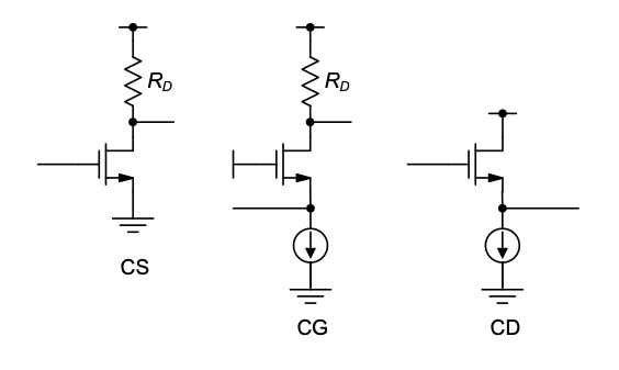
6.1.1 Voltage Amplifier
Recall that a voltage amplifier requires a high input resistance, a low output resistance, and (typically) a large voltage gain. From Chapter 2 we know that a common-source amplifier has an infinite input resistance since the MOS transistor has an insulating gate with no input current. Therefore, assuming that a common-source amplifier is the proper input stage for a voltage amplifier, we can explore cascading two of these stages to increase the voltage gain. The small-signal model of two cascaded common-source amplifiers is given in Figure 6.2.
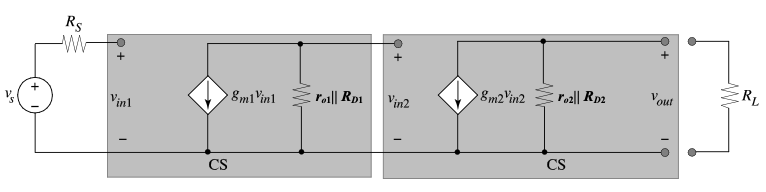
The input resistance of this cascade is infinite and the overall open-circuit voltage gain is given by the multiplication of the voltage gain of each stage as shown in
\[ A_v = g_{m1}(r_{o1}||R_{D1})g_{m2}(r_{o2}||R_{D2}) \tag{6.1}\]
The output resistance of this amplifier is
\[ R_{out} = r_{o2}||R_{D2} \tag{6.2}\]
This cascaded common-source voltage amplifier has two of the three required characteristics, namely a large input resistance and a high voltage gain. However, assuming that \(R_{D2}\) is reasonably large for high gain, it still has a high output resistance. This will degrade the voltage transfer from the amplifier to the load resistor.
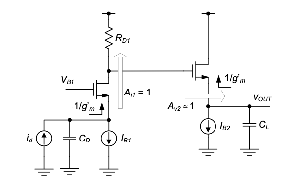
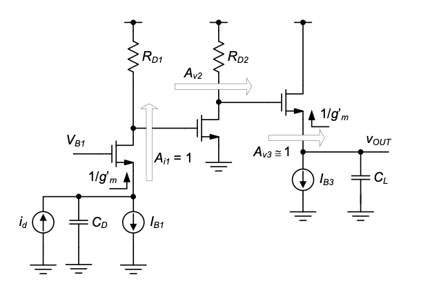
From Chapter 4 we know that a common-drain amplifier has an infinite input resistance, a low output resistance, and a voltage gain near unity (modeled as unity here for simplicity). We can cascade the small-signal, two-port model of a common-drain amplifier with the small-signal model of the common-source cascade described above. This three-stage amplifier is shown in Figure 6.3. As before, the cascaded common-source amplifiers are modeled with an infinite input resistance, a voltage gain \(A_v\), and an output resistance given by Equation 6.1 and Equation 6.2, respectively.
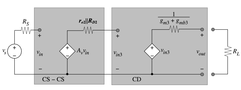
There is no interstage loss of voltage gain because the common-drain amplifier has infinite input resistance. In addition, the output resistance is reduced to approximately equal to the reciprocal of the transconductance plus the backgate transconductance of the common-drain amplifier. This usually gives a significant reduction in output resistance and allows this three-stage voltage amplifier to drive small load resistances while still maintaining a significant transfer of the open-circuit voltage to the load.
6.1.2 Transconductance Amplifier
A transconductance amplifier requires a large input resistance, a large transconductance, and a large output resistance to be able to pass most of its output current to the load. Let us explore using cascaded common-source amplifiers for a transconductance amplifier. In Figure 6.4 we show the small-signal model of two cascaded common-source amplifiers. We use the Norton equivalent output network since current is the output variable of interest. The short circuit transconductance of this amplifier is equal to
\[ G_m= \frac{i_{out}}{V_{in1}} = -g_{m1} (r_{o1}||R_{D1})g_{m2} = A_{v1}G_{m2} \tag{6.3}\]
Notice that the additional common-source stage increases the transconductance by the voltage gain of the first stage. There is no interstage loss since the input resistance to the second stage is infinite.
The output resistance of the transconductance amplifier is
\[ R_{out} =r_2 || R_{D2} \tag{6.4}\]
which is the output resistance of a single common-source amplifier stage.
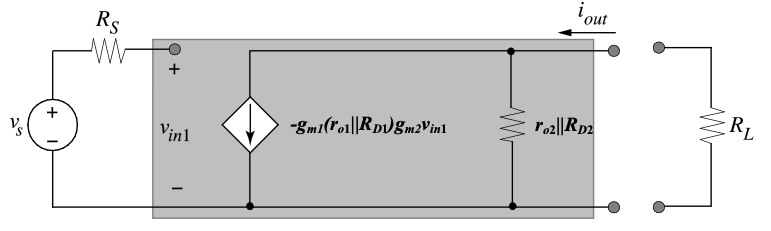
We can add a current buffer to increase the output resistance of the cascaded common-source amplifier. An ideal current buffer is defined as a circuit whose input resistance is very small, output resistance is very large, and has a current gain of unity. The common-gate amplifier studied in Chapter 4 is a good example of a current buffer. The small-signal model of a common-gate amplifier cascaded with two common-source amplifiers is shown in Figure 6.5.
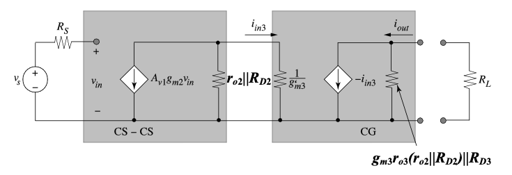
The output resistance is now
\[ R_{out} ≅ g_{m3}r_{o3}(r_{o2} || R_{D2}) || R_{D3} \tag{6.5}\]
Assuming that we can make RD3 negligibly large (by supplying the drain current using a long-channel, cascoded current source), the \(R_{out}\) is increased by \(g_{m3}r_{o3}\) with the help of the CG stage. The short circuit transconductance is given by
\[ G_m = \frac{i_{out}}{v_{in}} \]
\[ = -g_{m1}(r_{o1} \parallel R_{D1}) g_{m2} \left( \frac{r_{o2} \parallel R_{D2}}{r_{o2} \parallel R_{D2} + 1/g'_{m3}} \right) \]
\[ \equiv -g_{m1}(r_{o1} \parallel R_{D1}) g_{m2} \tag{6.6}\]
Note that the transconductance is only slightly degraded when compared to Equation 6.3 due to the parallel combination of the common-source output resistance with the common-gate input resistance. This degradation is negligible since the CG input resistance is small compared to the CS output resistance.
Example 6-1: Transresistance Amplifier
This example explores how to cascade two amplifier stages to form a transresistance amplifier. Select the stages and calculate \(R_{in}\), \(R_{out}\), and \(R_m\). Assume that the employed CS and CG stages (Figure 6.1) have drain resistors of value \(R_D << r_o\) in their output networks. Hint: Recall that a transresistance amplifier typically requires a low input resistance, a low output resistance, and a large transresistance.
SOLUTION
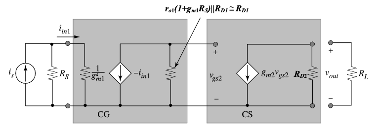
To obtain a low input resistance, we choose a CG amplifier as the first stage. The choice of the second stage depends on the specifications required. Let’s try a CS amplifier. The small-signal two-port model for a CG-CS cascade is shown in Figure 6.6 . \(R_{in}\) the input resistance, is \(1 / g'_m1\). \(R_{out}\), the output resistance, is equal to \(R_{D2}\). We need to find the unloaded (\(R_L \to \infty\)) transfer function between \(v_{out}\) and \(i_{in1}\) to calculate \(R_m\). We begin by writing
\[ v_{gs2} = i_{in1} R_{D1} \]
\[ v_{out} = -g_{m2} v_{gs2} R_{D2} \]
\[ R_m = \frac{v_{out}}{i_{in1}} = -g_{m2} R_{D1} R_{D2} \]
If we use a CD amplifier instead of a CS for the second stage, we expect a lower output resistance at the expense of lower transresistance. The small-signal two-port model for a CG-CD amplifier is shown in Figure 6.7, assuming for simplicity that the CD stage has unity voltage gain.
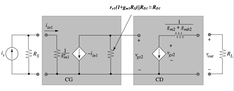
The input resistance is the same for both amplifiers since both use a CG stage as the input. The output resistance is \(R_{out} = \frac{1}{(g_{m2} + g_{mb2})}\). The transresistance \(R_m = \frac{v_{out}}{i_{in1}} = R_{D1}\) for the CG-CD configuration. Note that the output resistance and transresistance of the CG-CD configuration are lower than those of the CG-CS configuration by \(g_{m2} R_{D2}\). The proper topological choice depends on the specifications required and the relative value of \(R_L\) compared to \(R_{out}\).
6.2 High-Frequency Analysis
As we have already seen in our treatment of single-stage amplifiers, analyzing the frequency response of an amplifier by hand (as opposed to computer simulation) usually necessitates approximations. The approximations are needed not only to manage complexity, but also to gain intuition about the limiting components in the circuit. Clearly, as we cascade stages, this need for simplifying approximations becomes only stronger. In this section, we will examine typical strategies for the analysis of multistage amplifiers using two multi-stage amplifier examples: CG-CD and CS-CG (cascode amplifier). Our analysis of these circuits will heavily rely on the toolkit developed in Chapters 3 and 4 and will invoke concepts such as the method of open-circuit time constants and the Miller approximation.
6.2.1 OCT-Based Analysis of the CG-CD Cascade
We begin our discussion by considering the CG-CD transresistance amplifier shown in Figure 6.8(a), along with its small-signal model in Figure 6.8(b). The latter circuit is constructed by cascading the respective small-signal models from Chapter 4 (Figure 4.15 and Figure 4.24) and contains no approximations.
At least in principle, the exact frequency response of the model in Figure 6.8(b) can be found by writing KCL at the three nodes of the circuit, and solving a 3x3 system of equations to find \(V_{out}(s)/I_s(s)\). However, this procedure not only will be tedious, but will also produce long equations that are hard to interpret for design. Generally, accurate symbolic or numerical analysis of a large circuit is best left to a computer and is useful mainly to check our understanding and provide fine-tuned numerical answers. As circuit designers, we must always look for ways to simplify the circuit and consider only the main effects that set the performance metrics of interest. A first step to take in this direction is to simplify the small-signal model based on our understanding of the individual stages. In Figure 6.9, the following simplifications have been made:
◆ The resistance ro1 is omitted per the argument from Section 4-3-3. As long as \(R_{D1} << r_{o1}\), a unilateral model for the CG stage without ro1 is sufficiently accurate.
◆ The resistance \(r_{o2}\) is omitted since typically \(r_{o2} \gg 1 / g'_{m2}\).
◆ The capacitance \(C_{sb2}\) is omitted as discussed in Section 4-4-3. Due to the low output resistance of the CD stage, this capacitance will affect the behavior of the amplifier only at very high frequencies beyond our interest in a hand analysis.
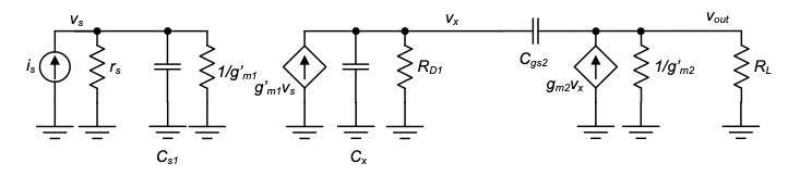
With these simplifications in place, the circuit has become much more manageable for hand analysis, but has the remaining issue that the second stage is bilateral due to \(C_{gs2}\). Again, while it is possible to analyze the circuit using KCL equations, the designer will typically look for further simplifications. These simplifications will now depend on the exact objective of the analysis. As a first example, suppose that we are only interested in obtaining a first-order estimate of the circuit’s bandwidth. In this case, applying the method of open-circuit time (OCT) constants is a suitable direction to take. As we have already seen in Chapter 4, the main advantage of an OCT-based analysis is that it breaks the overall task into manageable steps and simultaneously provides insight about bandwidth bottlenecks. We will reiterate this point in the following example.
Example 6-2: OCT Analysis of a CG-CD Transresistance Amplifier
Consider the CG-CD small-signal model of Figure 6.9 with the following parameters: \(g_{m1} = g_{m2} = 1\ \text{mS}\), \(g_{mb}/g_m = 0.2\), \(r_s = 50\ \text{k}\Omega\), \(R_{D1} = 10\ \text{k}\Omega\), \(R_L = 3\ \text{k}\Omega\), \(C_{s1} = 1\ \text{pF}\), \(C_x = 200\ \text{fF}\) and \(C_{gs2} = 200\ \text{fF}\). Estimate the circuit’s bandwidth using the method of open-circuit time constants.
Solution
First note that the two open-circuit time constants associated with \(C_{s1}\) and \(C_{d1}\) can be identified by inspection:
\[ \tau_{s1o} = C_{s1} \cdot \left( r_s \parallel \frac{1}{g'_m1} \right) = 0.82\ \text{ns} \]
\[ \tau_{1o} = C_{d1} \cdot R_{D1} = 2\ \text{ns} \]
Now, in order to find the Thévenin resistance associated with \(C_{gs2}\), we must consider a larger portion of the circuit, as shown below. Note that this setup resembles almost exactly the circuit of Figure 3.22, where we determined the Thévenin resistance for \(C_{gd}\) in a CS stage. The only difference here is that the sign of the controlled source is flipped, simply because the CD stage is non-inverting.
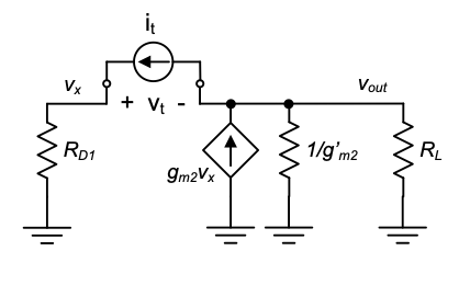
We can therefore directly apply the result of Equation 3.66: “\(R_{left} + R_{right} + g_m R_{left} R_{right}\)” but now with \(g_m\) replaced by \(-g_m\).
\[ R_{Tgs2} = R_{D1} + \left( R_L \parallel \frac{1}{g'_m2} \right) - g_{m2} R_{D1} \left( R_L \parallel \frac{1}{g'_m2} \right) \]
\[ = R_{D1} \left( 1 - g_{m2} \left( R_L \parallel \frac{1}{g'_m2} \right) \right) + \left( R_L \parallel \frac{1}{g'_m2} \right) \]
\[ = R_{D1}(1 - A'_{v20}) + \left( R_L \parallel \frac{1}{g'_m2} \right) \]
where \(A'_{v20} = v_{out} / v_x\) is the loaded voltage gain of the CD stage at low frequencies.
Note that the first term of the above expression accounts for the Miller gain across \(C_{gs2}\); we have already seen this term in our analysis of Section 4-4-3. Evaluating this result numerically, we find \(A'_{v20} = 0.652\) and \(R_{Tgs2} = 4.13\ \text{k}\Omega\), and thus:
\[ \tau_{gs2o} = C_{gs2} \cdot R_{Tgs2} = 0.826\ \text{ns} \]
\[ f_{3dB} \equiv \frac{1}{2\pi} \cdot \frac{1}{0.82\ \text{ns} + 2\ \text{ns} + 0.26\ \text{ns} + 0.826\ \text{ns}} = 43.7\ \text{MHz} \]
A simulation of the full circuit reveals \(f_{3dB} = 61\ \text{MHz}\). The OCT result is therefore off by about –26%, which is consistent with our understanding from Chapter 3. OCT bandwidth estimates are always conservative and tend to be off by 20–30% when there are several significant time constants.
6.2.2 Pole Calculations for the CG-CD Cascade\(^*\)
As indicated earlier, the OCT analysis above is useful as long as we are only interested in a first-order estimate of the circuit’s bandwidth. However, in some situations we may require knowledge of the circuit’s most significant poles and zeros. This would be the case, for example, if the amplifier was employed in a feedback system, where the exact location of the poles and zeros (rather than just the bandwidth estimate) play a significant role. While the analysis of feedback systems is beyond the scope of this module, it is worth introducing the reader to techniques suitable for pole-estimation in multi-stage circuits.
One typical approach that designers tend to follow for pole estimations is to try and approximate the circuit by a cascade of unilateral two-ports. As we have established in Section 3-4-4, for a cascade of unilateral two-ports with parallel RC sections, the circuit poles are directly set by the time constants at each port. Even though this strategy does not always give precise numerical results, it provides a great deal of intuition on how to influence the position of significant poles. We will now illustrate this approach using the CG-CD amplifier.
Example 6-3: Estimation of the Most Significant Poles in a CG-CD Transresistance Amplifier
Consider the CG-CD small-signal model of Figure 6.9 with the same parameters as in Example 6-2: \(g_{m1} = g_{m2} = 1\ \text{mS}\), \(g_{mb}/g_m = 0.2\), \(r_s = 50\ \text{k}\Omega\), \(R_{D1} = 10\ \text{k}\Omega\), \(R_L = 3\ \text{k}\Omega\), \(C_{s1} = 1\ \text{pF}\), \(C_x = 200\ \text{fF}\), and \(C_{gs2} = 200\ \text{fF}\). Estimate the locations of the circuit’s most significant poles.
Solution
In order to estimate the most significant poles without resorting to complex algebra, we construct a unilateral model for the CD portion of the circuit (as already established in Figure 4.29). The corresponding simplified circuit (shown in Figure 6.11) uses the Miller approximation to translate \(C_{gs2}\) into an equivalent parallel capacitance at the input port of the CD stage. This approximation is reasonable since in this example the voltage gain of the CD stage is constant up to very high frequencies, beyond the poles that we are trying to estimate.
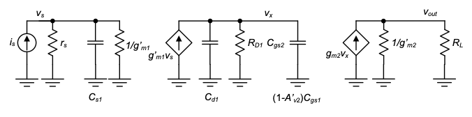
From the simplified circuit, we can immediately identify the approximate pole locations by inspection and write the complete circuit transfer function as
\[ p_1 = -\frac{1}{\left(r_s \parallel \frac{1}{g'_m}\right) C_{s1}} \]
\[ p_2 = -\frac{1}{R_{D1} \left[ C_{x} + \left(1 - A'_{v20}\right) C_{gs2} \right]} \tag{6.7}\]
\[ \frac{v_{out}}{i_s} = R_{m0} \cdot \frac{1}{1 - \tfrac{s}{p_1}} \cdot \frac{1}{1 - \tfrac{s}{p_2}} \]
where \(R_{m0} = R_{D1} A'_{v20}\) is the low-frequency transresistance. Evaluating the pole frequencies numerically, we find \(f_{p1} = 194 \,\text{MHz}\) and \(f_{p2} = 59 \,\text{MHz}\).
An accurate analysis of the full circuit reveals that there are three (real, LHP) poles and one (LHP) zero at the following respective frequencies: 67 MHz, 194 MHz, 1100 MHz, and 796 MHz (for the zero).
From the above example, we conclude that the simplified analysis has done a reasonable job at estimating the first two poles. This overall approach is very powerful, because it lets the designer quickly see which components set the most significant pole frequencies. For example, if we wanted to increase \(f_{p2}\), the result shows that reducing \(R_{D1}\) would be an option to consider.
Such guidance would have been harder to obtain from lengthy algebraic expressions that capture the complete circuit transfer function.
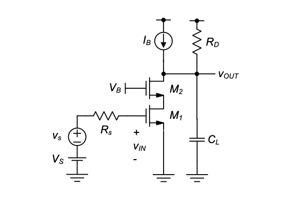
6.2.3 OCT-Based Analysis of the CS-CG Cascade (Cascode Amplifier)
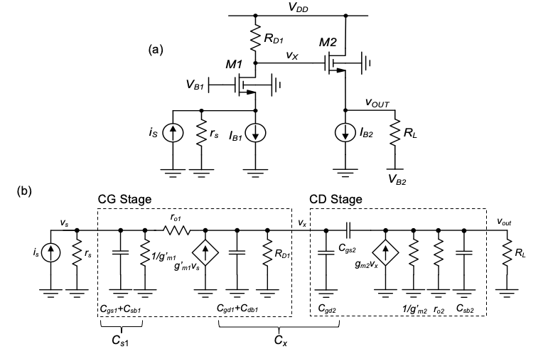
In this section, we explore the frequency response of another important multistage amplifier called the cascode amplifier. We have already briefly discussed this circuit in Section 4-5 and qualitatively argued that it should not suffer from the Miller effect, which often severely degrades the frequency response of the common-source amplifier. In the following discussion, we will analyze the frequency response of a cascode amplifier in the same spirit as we have done this in the previous section. That is, we will illustrate strategies that allow us to analyze and reason about the frequency response of the circuit intuitively, without much algebraic complexity.
For our analysis, we consider the circuit shown in Figure 6.12(a), along with its small-signal model in Figure 6.12(b). The shown model is complete, except that the output resistances of the two transistors have been neglected due to presence of the \(1/g_{m2}\) and \(R_D\) resistors (we assume \(1/g′_{m2} << r_{o1}\) and \(R_D << r_{o2}\)).
We begin by calculating the small-signal voltage gain of this amplifier at low frequencies by open-circuiting the capacitors.
This voltage gain is given by
\[ A_{v0} = \frac{v_x}{v_s} \cdot \frac{v_{out}}{v_x} = -\frac{g_{m1}}{g'_{m2}} \cdot g'_{m2} R_D = -g_{m1} R_D \tag{6.8}\]
Note that this is the same as the low-frequency voltage gain that is obtained from a common-source amplifier; the advantage of the cascode amplifier ies mainly in its wideband frequency response, as we will show next.
For a first-order estimate of the circuit’s bandwidth, we can consider its open-circuit time constants. Once again, we find the time constants by nspection, and using the
“\(R_{left} + R_{right} + g_m R_{left} R_{right}\)” rule to find the open-circuit time constant for \(C_{gd1}\).
\[ \tau_{gs1o} = R_s C_{gs} \tag{6.9}\]
\[ \tau_{xo} = \frac{C_x}{g'_{m2}} \tag{6.10}\]
\[ \tau_{gd1o} = \left[ R_S + \frac{1}{g'_{m2}} + g_{m1} R_S \frac{1}{g'_{m2}} \right] C_{gd1} \tag{6.11}\]
\[ = \left[ \frac{1}{g'_{m2}} + \left( 1 + \frac{g_{m1}}{g'_{m2}} \right) R_S \right] C_{gd1} \]
Next, we consider the time constant at the output node:
\[ \tau_{d2o} = R_D C_{d2s} \tag{6.12}\]
Thus, the bandwidth estimate of the stage is:
\[ \omega_{3dB} = \frac{1}{\tau_{gs1o} + \tau_{xo} + \tau_{gd1o} + \tau_{d2o}} \tag{6.13}\]
One key difference compared to a common-source amplifier lies in the time constant associated with \(C_{gd1}\). For the basic common-source amplifier in Chapter 3, we had
\[ \tau_{gdo} = \left[ R_D + (1 + g_m R_D)R_S \right] C_{gd} \tag{6.14}\]
which suffers from Miller amplification of the gate-drain capacitance by the factor \(g_m R_D\), which is the magnitude of the circuit’s DC voltage gain.
In contrast, no significant Miller amplification occurs in the cascode amplifier. Even if the cascode amplifier is designed for large overall voltage gain, the magnitude of the voltage gain across \(C_{gd1}\) is limited to \(g_{m1}/g'_{m2}\), which is typically close to unity. The following example looks at a numerical evaluation of this advantage.
Example 6-4: Cascode Amplifier Bandwidth Estimate Using an OCT Analysis
Consider the circuit shown in Figure Ex6-4 and assume the following component values: \(R_D = 5 \, k\Omega\), \(R_s = 50 \, k\Omega\) and for both MOSFETs: \(g_m = 1 \, \text{mS}\), \(C_{gs} = 40.7 \, \text{fF}\), \(C_{gd} = 10 \, \text{fF}\), \(C_{db} = C_{sb} = 11.6 \, \text{fF}\)
These are the same parameter values we used in Example 3-7, an OCT analysis of a basic CS amplifier. Assume that the body of \(M_2\) is connected to ground and that \(g_{mb2}/g_m = 0.2\).
Estimate the 3-dB bandwidth using an OCT analysis and compare the result to the bandwidth estimate of the original CS circuit from Example 3-7.
SOLUTION
Evaluating Equation 6.10 through Equation 6.13 numerically with the given values yields
\[ \tau_{gs1o} = 50k\Omega \cdot 40.7 \, \text{fF} = 2.035 \, \text{ns} \]
\[ \tau_{xo} = \frac{11.6 \, \text{fF} + 40.7 \, \text{fF} + 11.6 \, \text{fF}}{1 \, \text{mS}} = 64 \, \text{ps} \]
\[ \tau_{gd1o} = \left[ \frac{1}{1.2 \, \text{mS}} + \left( 1 + \frac{1 \, \text{mS}}{1.2 \, \text{mS}} \right) 50k\Omega \right] 10 \, \text{fF} = 925 \, \text{ps} \]
\[ \tau_{d2o} = 5k\Omega (10 \, \text{fF} + 11.6 \, \text{fF}) = 108 \, \text{ps} \]
The bandwidth estimate is therefore
\[ f_{3dB} = \frac{1}{2\pi} \cdot \frac{1}{2.035 \, \text{ns} + 64 \, \text{ps} + 925 \, \text{ps} + 108 \, \text{ps}} = 50.8 \, \text{MHz} \]
For comparison, the three time constants of the corresponding common-source amplifier (without \(M_2\)) would be (see Example 3-7, with \(C_L = 0\))
\[ \tau_{gso} = 50k\Omega \cdot 40.7 \, \text{fF} = 2.035 \, \text{ns} \]
\[ \tau_{db} = 5k\Omega \cdot 11.6 \, \text{fF} = 58 \, \text{ps} \]
\[ \tau_{gdo} = \left[ 5k\Omega + (1 + 1 \, \text{mS} \cdot 5k\Omega) 50k\Omega \right] 10 \, \text{fF} = 3.05 \, \text{ns} \]
and thus
\[ f_{3dB, \, CS} = \frac{1}{2\pi} \cdot \frac{1}{2.035 \, \text{ns} + 58 \, \text{ps} + 3.05 \, \text{ns}} = 30.9 \, \text{MHz} \]
The cascode amplifier’s bandwidth is about 62% larger than that of the basic common-source voltage amplifier, which is a significant improvement.
6.2.4 Pole Calculations for the CS-CG Cascade (Cascode Amplifier)\(^*\)
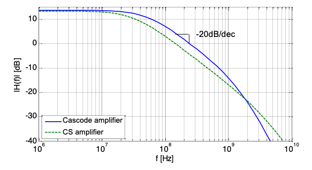
While the bandwidth increase seen in Example 6-4 is a welcome feature of the cascode amplifier, it comes with the issue that an additional pole is introduced. This is illustrated in Figure 6.14, which shows a computer simulation of he frequency response for both circuits considered in Example 6-4. The cascode amplifier has a larger 3-dB corner frequency, but exhibits an extra pole that bends the response more sharply at high frequencies. In many cases this behavior is not troublesome. However, it turns out that these non-dominant poles must usually be considered in feedback amplifiers and often limit performance. Consequently, there is a general need for the circuit designer to be able to calculate the location of the high-frequency poles in a cascode amplifier.
There are several ways by which one can estimate the location of the poles for the cascode amplifier. The most appropriate method is to invoke the expressions we have already derived in Chapter 3 for the dominant and non-dominant pole of a CS amplifier. Specifically, we note that the left portion of the model in Figure 6.12(b) is equivalent to the CS amplifier analyzed in Chapter 3 (Figure 3.15) with the following variable changes: \(C_{db} \to C_x\) and \(R_{out} \to 1 / g_m^{\prime 2}\).
With these substitutions, the dominant pole frequency is most concisely written using the Miller approximation result from Equation 3.56, which becomes
\[ \omega_{p1} = \frac{1}{R_s \left[ C_{gs1} + \left( 1 + \frac{g_{m1}}{g_m^{\prime 2}} \right) C_{gd1} \right]} \tag{6.15}\]
From this expression, we immediately see that the dominant pole does not suffer from significant Miller multiplication. This is analogous to the improvement we have seen in the zero value time constant of \(C_{gd1}\).
An expression for the second pole frequency was derived in Eq. (3.56), which in the present context becomes
\[ \omega_{p2} \cong \frac{g_m^{\prime 2}}{C_x} + \frac{1}{R_s C_{gs1}} + \frac{g_{m1}}{C_x} \cdot \frac{C_{gd1}}{C_{gs1}} \tag{6.16}\]
For the particular example that we consider here, we know that \(R_s C_{gs1} \gg C_x / g_m^{\prime 2}\). Also, since \(g_{m1}\) and \(g_m^{\prime 2}\) are typically comparable and \(C_{gd1} \ll C_{gs1}\), we can drop all but the first term in Equation 6.16 to obtain
\[ \omega_{p2} \cong \frac{g_m'}{C_x} \quad \tag{6.17}\]
Since \(C_x\) is usually dominated by the gate capacitance of \(M_2\) (\(C_{gs2}\)), \(\omega_{p2}\) is typically close to the transistor’s transit frequency \((g_{m2}/C_{gg2})\). For a minimum length n-channel device in our technology, this frequency is on the order of 1 GHz for typical biasing conditions (see Chapter 3).
Finally, we can easily identify the third pole frequency of the cascode amplifier directly from Figure 6-8(b). The RC network at the output branch is unilaterally coupled to the CS amplifier portion and therefore contributes a pole corresponding the branch’s parallel RC time constant.
\[ \omega_{p3} \cong \frac{1}{R_D C_{d2}} \quad \tag{6.18}\]
From these pole frequency expressions, we see that the cascode amplifier can be conveniently modeled as shown in Figure 6-10. We have thus once again arrived at a relatively simple and intuitive unilateral model that captures most of the relevant ircuit behavior, and specifically the circuit’s pole locations. It can be shown that this model is still valid for scenarios where the dominant pole is not at the input, but instead associated with the output of the circuit.
Example 6-5: Pole Calculations for a Cascode Amplifier
Compute the pole frequencies for the cascode amplifier considered in Example 6-4 (Figure 6.13). The parameters are: \(R_D = 5k\Omega, R_S = 50k\Omega\), and for both MOSFETs: \(g_m = 1 \,\text{mS}, \quad C_{gs} = 40.7 \,\text{fF}, \quad C_{gd} = 10 \,\text{fF},\)
\(C_{db} = C_{sb} = 11.6 \,\text{fF}, \quad \text{and } g_{mb}/g_m = 0.2.\)
SOLUTION
Evaluating Equation 6.15, Equation 6.17, and Equation 6.18 numerically gives
\[ f_{p1} = \frac{1}{2 \pi} \cdot \frac{1}{50k\Omega \left[ 40.7 \,\text{fF} + \left(1 + \frac{1\,\text{mS}}{1.2\,\text{mS}}\right) 10\,\text{fF} \right]} = 53.9 \,\text{MHz} \quad \]
\[ f_{p2} \cong \frac{1.2\,\text{mS}}{2 \pi (40.7\,\text{fF} + 11.7\,\text{fF} + 11.7\,\text{fF})} = 3.0 \,\text{GHz} \quad \]
\[ f_{p3} \cong \frac{1}{2 \pi (5k\Omega)(10\,\text{fF} + 11.7\,\text{fF})} = 1.47 \,\text{GHz} \quad \]
Note that these pole frequencies correspond to the magnitude response that was shown in Figure 6.14. There is one dominant pole, and two non-dominant poles beyond 1 GHz.
6.3 Design of a Three-Stage Transresistance Amplifier
In this section we will explore the design and optimization of a three-stage transresistance amplifier for use in a fiber optic receiver. The objective is to illustrate the process that a designer faced with this problem would have to go through. Furthermore, we present a systematic approach for the sizing of the amplifier components to achieve near-optimum performance under a given set of constraints.
6.3.1 Problem Definition
As illustrated in Figure 6.15, we wish to amplify the signal delivered from a photodiode over a wide bandwidth and drive this amplified signal into a capacitive load. The overall specifications for the problem are summarized in Table 6-1.
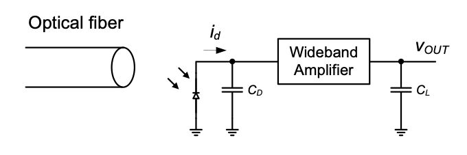
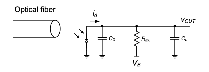
In order to appreciate why an amplifier is needed in the first place to solve this problem, let us consider the “trivial” solutions shown in Figure 6.16. Interestingly, if all we did was to connect a resistance of value \(R_{m0}\) to the diode, we would already meet the low-frequency transresistance specification of the circuit without using any transistors (\(v_{out}/i_d = R_{m0}\)).
However, the key issue then is that we would not be able to achieve high bandwidth. In this solution, the bandwidth is only
\[ \frac{1}{2 \pi R_{m0}(C_L + C_D)} = 5.3 \,\text{MHz} \]
We will be able to do better with an active circuit.
| Parameter | Symbol | Value |
|---|---|---|
| Low Frequency Transresistance | \(R_{m0}\) | 2 k\(\Omega\) |
| Load Capacitance | \(C_L\) | 10 pF |
| Diode Capacitance | \(C_D\) | 5 pF |
| Total Drain Current | \(I_{Dtot}\) | 3 mA |
| Bandwidth | \(f_{3dB}\) | Maximize |
6.3.2 Circuit Architecture Considerations
In order to achieve high bandwidth, we must ensure that the large capacitors at the input and output of the circuit “see” low resistances, such that their presence does not create large time constants. Based on we have learned in this module, one possible solution is to employ a CG stage at the input and a CD stage at the output of the circuit. This option is shown in Figure 6.17, where we have qualitatively annotated the signal flow and relevant gain terms and port resistances in the circuit. A representation of this style is sometimes used by experienced designers who are already familiar with the small-signal model of each stage, and usually won’t bother to draw it out. We use this representation here and in the following figures to prepare the reader toward this transition.
Here, \(CD\) is presented with the low input resistance of the CG stage and \(C_L\) sees the low output resistance of the CD buffer. In terms of signal flow, the CG stage acts as a current buffer and passes \(i_d\) essentially unchanged to \(R_{D1}\). The resistor \(R_{D1}\) performs a current-to-voltage conversion that corresponds to the desired transresistance, while the CD stage buffers the generated voltage to handle the large load capacitance \(C_L\).
This proposed circuit would in principle work but contains one significant challenge. Essentially, all of the transresistance is due to \(R_{D1}\), which must therefore be set to approximately \(2 kΩ\). Together with the input capacitance of the CD stage, this resistor creates a time constant that may dominate the circuit and may again not allow us to achieve large bandwidth. A typical remedy to this problem is to do a better job at distributing the gain among several stages of the amplifier. One such option is shown in Figure 6.18. Here, we employed a basic CS voltage amplifier between the CG and CD stages. Since the CS stage will have voltage gain, the resistance \(R_{D1}\) can be reduced by this gain factor to achieve the same overall transresistance. This will reduce the time constants that are proportional to \(R_{D1}\) and therefore help maximize the bandwidth.
An additional improvement that could be considered in this circuit is to use a cascode amplifier rather than simple CS stage to implement the gain stage (see Reference 1). This would help to reduce the capacitance seen by \(R_{D1}\) and therefore speed up the circuit. For simplicity, we will not pursue this idea and instead work with the circuit of Figure 6.18 toward a final solution. The reader is invited to explore using a cascode stage for improved performance.
6.3.3 Biasing Considerations
As we have seen in Chapters 2 and 5, biasing a common-source stage properly can be a difficult task. One issue in the prototype circuit of Figure 6.18 is that any parameter variation in \(I_{B1}\) or \(R_{D1}\) will directly impact the quiescent point voltage at the gate of the CS stage. Since this stage has voltage gain, such variations will then show up amplified at its output and potentially drive parts of the circuit out of saturation and/or limit the available signal swing.
To overcome this issue, we employ the replica biasing approach introduced in Chapter 5 (see Figure 6.19). Here, the bias point at the gate of \(M_2\) is set via the replica device \(M_2\). This diode-connected transistor is biased with the same current as \(M_2\), and thereby “computes” the correct bias voltage that will also track threshold voltage process variations. Also, this voltage is to first-order independent of variations in \(I_{B1}\) and \(R_{D1}\). As long as \(I_{B1a}\) and \(I_{B1b}\) match, these currents can vary in their absolute value without disturbing the bias point of \(M_2\). Similarly, the bias point of \(M_2\) is not disturbed by changes in the value of \(R_x\), since this resistor (to first-order) carries no current at the quiescent point.
At the drain side of \(M_2\), we employ a resistive divider to set the bias point gate potential for \(M_3\). In this arrangement, the division ratio can be adjusted for the proper input bias voltage for the CD stage (e.g., \(V_{DD}/2\)), and the absolute resistor value is determined by the desired gain of the CS stage (the \(g_{m2}R_{D2}\) product).
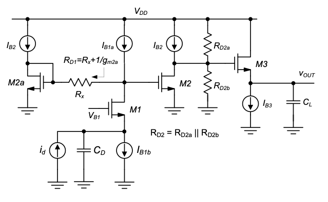
The current sources required in Figure 6.19 can be realized using the current mirror circuits discussed in Chapter 5, and supplied for example by a globally shared constant-\(g_m\) reference current source. A variety of options exists for the generation of the CG bias voltage \(V_{B1}\). This voltage can be set up by one of the two methods shown in Figure 5.28. Without further working through the details required to complete the bias circuit, we will now investigate a proper procedure for sizing the ignal path devices.
6.3.4 Examination of Tradeoffs
To complete our design, we must determine all bias currents, transistor geometries and resistor values. As we shall see, this is a non-trivial task, especially if we want to achieve optimum performance, as for instance maximum bandwidth in the given problem. Even though the circuit has only three transistors, there are several degrees of freedom among the different design variables.
A first step in the right direction is to begin and identify the relationships that govern the performance of the circuit and analyze these for the key tradeoffs. Furthermore, in this process, we must make reasonable approximations to keep the algebraic
To keep the algebraic complexity low, let us begin by writing an expression for the circuit’s low-frequency transresistance.
\[ R_{m0} = R_{D1} A_{v20} A_{v30} \equiv -R_{D1} \cdot g_{m2} R_{D2} \cdot \frac{g_{m3}}{g_{m3}^\prime} \tag{6.19}\]
Since the last term in Equation 6.19 is close to unity, it is clear that \(R_{m0}\) is primarily set by the product of \(R_{D1}\) and the CS stage voltage gain. Now, since we are only interested in the circuit’s bandwidth, and not the exact pole/zero locations, using an OCT estimate for further analysis is most appropriate and convenient.
The schematic in Figure 6.20 includes all of the relevant capacitances that give rise to time constants. Several of the indicated capacitances are parallel combinations and for simplicity it is important to immediately discard small capacitances that may not impact the design significantly. For instance, we neglect \(C_{sb1}\) relative to the large diode capacitance at the input node. In addition, we neglect several other extrinsic capacitances that should limit the bandwidth significantly.
Once the design is completed, all of these assumptions can be checked, for instance through a computer simulation of the full circuit. By inspection, we identify the following six open-circuit time constants.
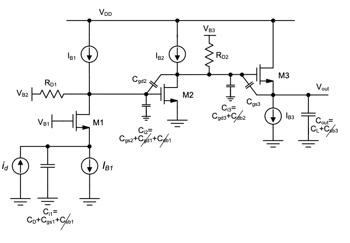
\[ \tau_{i1o} = \frac{C_D + C_{gs1}}{g_m^{\prime}1} \]
\[ \tau_{i2o} = R_{D1}C_{gs2} \]
\[ \tau_{gd2o} = (R_{D1} + R_{D2} + g_{m2}R_{D1}R_{D2})C_{gd2} \tag{6.20}\]
\[ \tau_{i3o} = R_{D2}C_{gd3} \]
\[ \tau_{gs3o} = \left(R_{D2} + \frac{1}{g_m^{\prime}3} - \frac{g_{m3}}{g_m^{\prime}3}R_{D2}\right)C_{gs3} \]
\[ \tau_{outo} = \frac{C_L}{g_m^{\prime}3} \]
where we have again made use of the “\(R_{left} + R_{right} \pm g_mR_{left}R_{right}\)” rule to find \(\tau_{gd2o}\) and \(\tau_{gs3o}\). Now, since \(R_{D1}\) and \(R_{D2}\) are among the key parameters that set the overall transresistance, it makes sense to collect the respective proportional terms in Equation 6.20.
\[ \tau_{core} = R_{D1}(C_{gs2} + [1 + g_{m2}R_{D2}]C_{gd2}) \\ + R_{D2}\left(C_{gd3} + \left[1 - \frac{g_{m3}}{g_m^{\prime}3}\right]C_{gs3}\right) \tag{6.21}\]
We call this time constant \(\tau_{core}\), since it is associated with the resistors in the core of the overall amplifier.
To gain further insight into the tradeoffs dictated by this expression, we can rewrite as \[ \tau_{core} = \frac{R_m}{|A_{v20}| A_{v30}} \big(C_{gs2} + [1 + |A_{v20}|]C_{gd2}\big) + \frac{|A_{v20}|}{g_{m2}} \big(C_{gd3} + [1 - A_{v30}]C_{gs3}\big) \tag{6.22}\]
From this formula, we see that one part of the time constant increases with \(A_{v20}\), while the other component decreases. This suggests that choosing the right amount of voltage gain may be key to maximizing the bandwidth. As far as the remaining terms of Equation 6.20 are concerned, it makes sense to group these together in a similar fashion; that is, to collect terms for the input and output network, respectively.
\[ \tau_{in} = \frac{C_D + C_{gs1}}{g'_ {m1}} \tag{6.23}\] \[ \tau_{out} = \frac{C_L + C_{gs3}}{g'_{m3}} \tag{6.24}\]
At first glance, these expressions do not provide any interesting opportunity for tradeoffs.
Given our finite budget for drain current, the amount of \(g_m\) we can generate will be limited, and this will essentially set \(\tau_{in}\) and \(\tau_{out}\). The main degree of freedom here is what fraction of the available current we are going to use in the input and output branches.
6.3.5 Optimization Procedure
Given the above observations, the key question that remains is how we should distribute the available current among the three amplifier stages. There are several ways in which we can perform this optimization. One would be to immediately engage in circuit simulations and iterate over current distributions and device geometries until we have identified a satisfactory answer. This approach, however, not only is time-consuming, but also gives little insight about the quality and robustness of the obtained design point. The other extreme would be to try to formulate a closed form expression for the optimal sizing. Unfortunately, for all but the most trivial circuits this turns out to be impossible or infeasible.
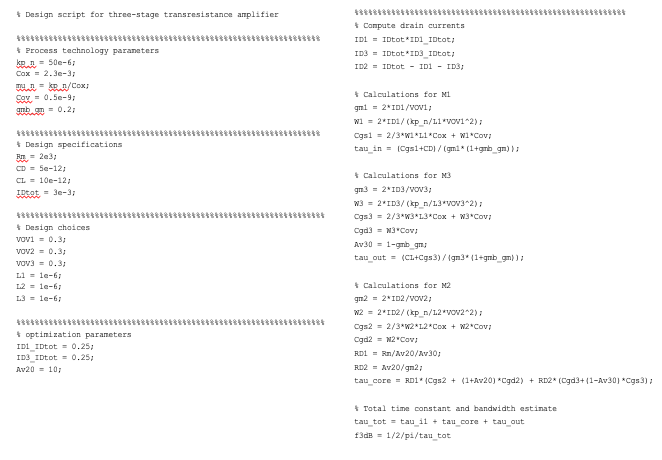
An approach that lies about midway between these extremes is to set up an insight-based, hand-crafted calculation script that allows the designer to quickly sweep through the design space by specifying a few reasonable assumptions and exercising the key “knobs” that control the tradeoffs. For example, as we have explained above, one such knob in our design is the voltage gain of the CS stage. Figure 6.21 shows one possible way of setting up a calculation script for our design problem. The script contains five distinct sections:
◆ The definition of process technology parameters such as \(\mu_n C_{ox}\), etc. Here, we can also define first-order estimates that may be needed in the calculations—for instance, a typical value for \(g_{mb} / g_m\).
◆ The design specifications (desired \(R_{m0}, C_L\), etc.).
◆ A set of design choices that represent reasonable guess values for some of the unknowns that are not expected to play a significant role in the optimization or that we want to fix to specific values. For instance, in the shown script we set all channel lengths to minimum length (for high speed) and set all gate overdrive voltages to a typical value of 0.3 V. The latter choice could be imposed r instance by linearity or signal swing requirements. These parameters can, of course, be changed in the design process, but are not viewed as the main degrees of freedom.
◆ The main variables, which are the voltage gain of the CS stage (\(A_{v20}\)) and the allocation of current for the input and output branches (\(I_{D1}/I_{Dtot}\) and \(I_{D3}/I_{Dtot}\)). These are the primary knobs that we wish to adjust to search for optima.
◆ The performance and sizing calculations based on the given design choices and values set for the main variables. The output of this part is essentially the objective function of the optimization, which is bandwidth (or the total sum of the time constants) in our example.
Once such a script has been generated, it is straightforward to explore the design space and adjust the main variables to find a suitable design point. This can be done manually, or automatically using for loops. Figure 6.22 shows a plot that was generated by sweeping the CS stage’s gain while leaving the current allocations for input branches at the values indicated in Figure 6.21. This plot shows the existence of an optimum that we had already suspected from Equation 6.22: one part of the amplifier core’s time constant increases with \(A_{v20}\), while the other component decreases. Given our process parameters, specifications and design choices, the best value for the CS voltage gain is in the range of 10–20. Similar sweeps can be performed with the other variables to arrive at a final design point that is acceptable.
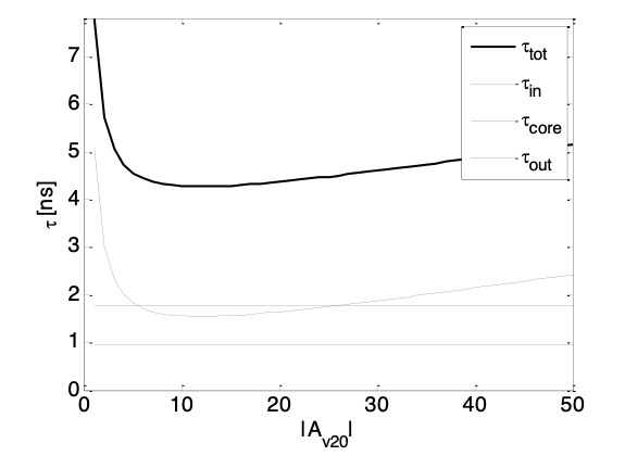
Interestingly, the tradeoff curve in Figure 6.22 exhibits a rather shallow optimum. This is a quite typical and welcome feature in circuit design problems. Anything but a shallow optimum would make us wonder whether the chosen point would be robust in presence of PVT variations and mismatch. A clear advantage of working with a design script (as opposed to repetitive simulation) is that we can visualize the region surrounding the chose design point.
6.3.6 Performance Verification
Even though the circuit simulator is not the best tool for optimization, it is the ultimate tool for verifying the circuit’s performance and to track down discrepancies due to simplifications in made in the design script. Once we have determined all parameters in our design script, we can use the computed currents and transistor geometries as input for a simulation that is based on the complete circuit and full transis tor models. As an example, we consider here the design point summarized in Table 6-2.
| Parameter | Symbol | Value |
|---|---|---|
| Fractional input branch current | \(I_{D1}/I_{Dtot}\) | 0.25 |
| Fractional output branch current | \(I_{D3}/I_{Dtot}\) | 0.25 |
| CS Stage voltage gain | \(|A_{v20}|\) | 10 |
| Width of \(M_1\) | \(W_1\) | 333 μm |
| Width of \(M_2\) | \(W_2\) | 666 μm |
| Width of \(M_3\) | \(W_3\) | 333 μm |
| Drain resistance of CG stage | \(R_{D1}\) | 250 Ω |
| Drain resistance of CS stage | \(R_{D2}\) | 1 kΩ |
| Total time constant | \(\tau_{tot}\) | 4.16 ns |
| Bandwidth estimate | \(f_{3dB}\) | 38.2 MHz |
A computer simulation of the full circuit with the above geometries, currents and resistor values shows
\(R_{m0} = 2.13 \, \text{k}\Omega \quad \text{and} \quad f_{3dB} = 70 \, \text{MHz}.\)
The corresponding errors in the design script values are −6.5% and −45%, respectively. The majority of the error in the $f_{3dB}$ estimate is systematic and due to the conservative nature of OCT bandwidth estimates (see Chapter 3).
The remaining percent differences can be tracked down to a slightly higher than desired $I_{D2}$ in the actual circuit due to channel length modulation (which can be significant at minimum length). This and other discrepancies can usually be explained and either resolved or properly incorporated in the design script and do not negatively interfere with the proposed optimization flow.
Quite contrary, comparing and resolving discrepancies between the script and simulation improve insight and lead to a form of “double book keeping” in the design flow that helps prevent erroneous design outcomes.
Finally, it is important to note that in addition to the discussed verification of small-signal performance, the circuit must always be simulated under large-signal (transient) conditions for the ultimate performance check.
6.3.7 Considerations for Advanced Technologies
The above-discussed example provided a framework for circuit design with square-law equations. A significant, but not insurmountable, hurdle that must be overcome when applying this approach with modern CMOS technologies lies in the growing complexity of transistor models. The latest generation of short-channel MOSFET models is based on hundreds of modeling parameters, a complexity that is manageable by a computer, but not practical for hand calculations and direct scripting. A solution to this problem that fits seamlessly into the proposed flow is to replace the square-law equations with computer generated look-up tables that relate the transistor parameters of interest numerically. An example is a look-up table that relates the gate-overdrive voltage to the transconductance per unit width of a MOSFET. Suitable ways to parameterize and use such tables are discussed in advanced literature on this subject, see for example References 2 and 3.
6.4 Summary
In this chapter, we discussed the analysis and design of multistage amplifiers. The small-signal two-port models were used to investigate the use of various types of amplifiers to transform the input or output resistance as well as increase the gain (voltage, current, transconductance, transresistance). Next, we analyzed two important examples of two-stage amplifiers in terms of their frequency response. We ended the chapter with a design of a transresistance amplifier to apply the concepts studied in this module. Specifically, we showed
◆ How to use the two-port models to find a quick approximation of the overall amplifier performance at low frequencies.
◆ How to approach the high-frequency analysis of multistage amplifiers using OCT bandwidth estimates and unilateral two-port models for the quick extraction of significant pole frequencies.
◆ How to design a larger circuit systematically, with the help of insight-based design scripts.
6.5 References
Y. Shim et al., “Design of Full Band UWB Common-Gate LNA,” IEEE Microwave and Wireless Components Letters, vol. 17, no. 10, pp. 721–723, Oct. 2007.
P. Jespers, The \(gₘ/I_D\) Methodology, a sizing tool for low-voltage analog CMOS Circuits, Springer, 2010.
T. Konishi, K. Inazu, J.G. Lee, M. Natsui, S. Masui, and B. Murmann, “Design Optimization of High-Speed and Low-Power Operational Transconductance Amplifier Using \(gₘ/I_D\) Lookup Table Methodology,” IEICE Trans. Electronics, vol. E94-C, no. 3, pp. 334–345, March 2011.
6.6 Problems
Unless otherwise stated, use the standard model parameters specified in Table 4-1 for the problems given below. Consider only first-order MOSFET behavior and include channel-length modulation (as well as any other second-order effects) only where explicitly stated.
P6.1 This problem compares a CS-CS voltage amplifier with a CS-CD voltage amplifier. If you are given that the \(g_m\) of the MOS devices is 1 mS and \(r_o\) is 100 k \(\Omega\) (assume that \(R_D\) is infinite), which topology yields the highest overall voltage gain, given
\(R_S = 1 \, \text{k}\Omega\) and \(R_L = 100 \, \Omega\)
\(R_S = 1 \, \text{k}\Omega\) and \(R_L = 10 \, \text{k}\Omega\)
Repeat (a) and (b) when \(g_m = 100 \, \mu S\) and \(r_o = 10 \, \text{M}\Omega\)
P6.2 This problem compares a CS-CS transconductance amplifier with a CS-CG transconductance amplifier. If you are given that the \(g_m\) of the MOS devices is 1 mS and \(r_o\) is 100 k\(\Omega\) (assume that \(R_D\) is infinite), which topology gives the highest overall transconductance, given
\(R_S = 1 \, \text{k}\Omega\) and \(R_L = 100 \, \Omega\)
\(R_S = 1 \, \text{k}\Omega\) and \(R_L = 10 \, \text{k}\Omega\)
Repeat (a) and (b) when \(g_m = 100 \, \mu S\) and \(r_o = 10 \, \text{M}\Omega\)
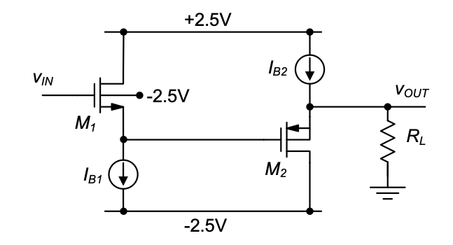
P6.3 A voltage buffer is shown in Figure 6.23. We have assumed that the circuit is fabricated in an n-well CMOS process where we can short the back-gate and source of the p-channel device. Parameters:
\(I_{B1} = I_{B2} = 200 \, \mu A\), \((W/L)_1 = (W/L)_2 = 50\). Neglect channel-length modulation.
What is \(V_{OUT}\) given \(V_{IN} = 0 \, V\)?
Find the open-circuit voltage gain (\(R_L \to \infty\)).
What is the minimum load resistor that the amplifier can drive and still maintain a voltage gain of 0.6?
P6.4 Repeat P6.3 given that the circuit is fabricated in a p-well CMOS process and that the n-channel device has its backgate shorted to the source and the p-channel device has its backgate tied to the positive power supply.
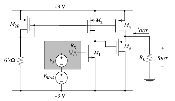
P6.5 You are given the voltage amplifier shown in Figure 6.24 with \((W/L)_1 = 20\) and \((W/L)_3 = 50\). In this problem we will assume (for simplicity) that all backgates are shorted to their respective source terminals. Neglect channel-length modulation.
Find the \(W/L\) for \(M_2\), \(M_{2B}\), and \(M_4\) (same for all three transistors) so that each MOSFET has a drain current of \(500 \,\mu A\).
What is the required voltage at the gate of \(M_3\) so that the output level will be 0 V?
Calculate \(V_{BIAS}\) so that \(M_1\) sinks the current from \(M_2\).
Draw a two-port model of this CS–CD stage and calculate the parameters.
Calculate the overall voltage gain if \(R_S = 10 \, \text{k}\Omega\) and \(R_L = 1 \, \text{k}\Omega\).
P6.6 A cascode transconductance amplifier is shown in Figure 6.25. Neglect the backgate effect for this problem.
Calculate \((W/L)_1\) of \(M_1\) such that the small-signal transconductance, \(i_{out}/v_s = 1 \, \text{mS}\). Assume \(R_L = 0 \, \Omega\) (short-circuit output current) for this part.
Calculate the value of \(V_{BIAS}\) using the \((W/L)_1\) calculated in part (a) such that \(I_{OUT} = 0 \, A\).
Calculate the output resistance of this transconductance amplifier.
Calculate the overall transconductance at DC given that \(R_S = 10 \, k\Omega\) and \(R_L = 1 \, k\Omega\).
Estimate the bandwidth of this circuit given that \(R_S = 10 \, k\Omega\) and \(R_L = 1 \, k\Omega\).
P6.7
In this problem we will investigate an interesting case in which the benefit of cascoding is dependent upon operating frequency. In the cascode amplifier shown in Figure 6.26, all devices are biased in the saturation region. You may neglect backgate effect, but you must include finite output resistance (\(r_o\)) of \(M_1\). Neglect all device capacitances, and consider only the explicitly shown \(C_L\). Simplify your analysis by assuming \(g_m r_o \gg 1\).
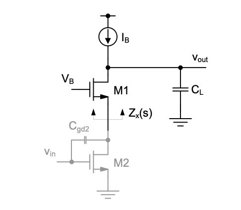
Derive an analytical expression for the impedance \(Z_x(s)\) looking into the source of \(M_1\) in terms of small-signal device parameters and \(C_L\).
Sketch \(|Z_x(j\omega)|\) versus frequency using logarithmic scales on both axes. Mark pertinent breakpoints symbolically, using the involved circuit parameters.
Explain in a few words for which frequency range M1 helps alleviate the Miller multiplication of \(C_{gd2}\).
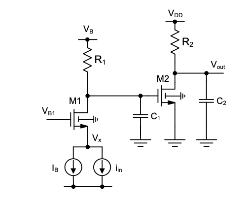
P6.8 In the transresistance amplifier shown in Figure 6.26, all devices operate in the saturation region. Neglect channel-length modulation in all parts of this problem.
After building this circuit in the lab, you measure \(V_X = 1 \text{ V}\) at the operating point. What is the corresponding value of the bias current \(I_B\)? In this calculation, be sure to consider the back-gate effect. Given parameters: \(W_1 / L_1 = 20\), \(V_{BI} = 2.5 \text{ V}\).
Assuming that the transresistance \(R_m = v_{out} / i_{in}\) is equal to \(50 \text{ k}\Omega\), compute the values of \(R_1\) and \(R_2\) that minimize \(\tau_{tot}\), the sum of all open-circuit time constants in the circuit. In this calculation, ignore all capacitances other than the explicitly drawn \(C_1\) and \(C_2\). Given parameters: \(g_{m2} = 2 \text{ mS}\), \(C_1 = 1 \text{ pF}\), \(C_2 = 2 \text{ pF}\).
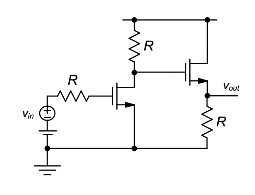
P6.9 In the amplifier circuit shown in Figure 6.28, ignore finite output resistance, extrinsic device capacitances and the backgate effect. Both transistors operate in the saturation region. Parameters: \(g_m = 5 \text{ mS}\), \(f_T = 5 \text{ GHz}\), \(R = 1 \text{ k}\Omega\). Calculate:
The amplifier’s small signal gain \(v_{out} / v_{in}\) at low frequencies (ignore all capacitances). Be sure to include the appropriate sign.
The amplifier’s 3-dB bandwidth using the open-circuit time constant method.
P6.10 Consider the cascode amplifier from Example 6-4. Assuming the same parameters values for \(M_1\) and all other components, we are interested in finding out how varying the width of \(M_2\) affects the OCT bandwidth estimate.
Recalculate the OCT bandwidth estimate assuming that the width of \(M_2\) has been doubled.
Recalculate the OCT bandwidth estimate assuming that the width of \(M_2\) has been halved.
P6.11 Consider the cascode amplifier from Example 6-5. Assuming the same parameters values for \(M_1\) and all other components, we are interested in finding out how varying the width of \(M_2\) affects the pole frequencies.
Recalculate the pole frequencies assuming that the width of \(M_2\) has been doubled.
Recalculate the pole frequencies assuming that the width of \(M_2\) has been halved.
P6.12 Consider the cascode amplifier with replica biasing shown in Figure 6.29. In this circuit, \(M_0\) and \(M_1\) are identical and have \(W/L = 4\). For \(M_3\), assume that \(L_3 = nL\), that is, the length for \(M_3\) is increased by a factor of \(n\) relative to \(M_1\) and \(M_2\). Ignore channel-length modulation throughout this problem.
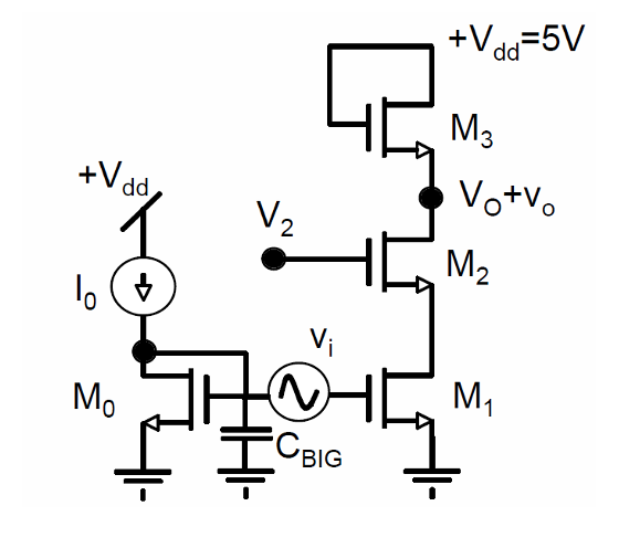
For \(n = 2\) and \(I_0 = 50 \, \mu A\), determine the minimum and maximum values for \(V_O\) and \(V_2\) in the quiescent point so that all transistors remain saturated. Ignore the backgate effect in this part of the problem.
Repeat part (a) taking the backgate effect into account.
Assuming that the devices are all operating in saturation, write a symbolic expression for the circuit’s low-frequency small-signal voltage gain in terms of \(g_m\) and \(g_{mb}\). Compute this voltage gain numerically.
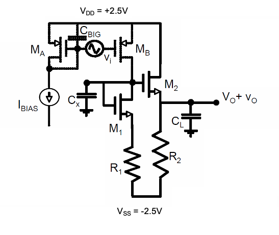
P6.13 Consider the CS-CD amplifier shown Figure 6.30. In this problem we will consider a biasing technique used to address PVT variation issues and will look at ways to optimize this circuit using a design script. All devices in the circuit can be assumed to have \(L = L_{min} = 1 \, \mu m\). The resistor \(R_1\) and transistor \(M_1\) serve as an input bias circuit for the CD stage and also as the drain resistance for the CS stage. To make the circuit robust against PVT variations, we impose the constraint \(\frac{I_{D2}}{I_{D1}} = \frac{R_2}{R_1} = \frac{W_2}{W_1} = n.\)
Assume that \(I_{BIAS} = 100 \, \mu A\) and that \(n = 3\). Additionally, assume \(W_A = W_B = 16 \, \mu m\) and \(W_1 = 9 \, \mu m\). Also, initially you can neglect finite \(r_o\) and backgate effect. By design, we want \(V_O\) to be 0 V in the quiescent point. Determine the gate overdrive voltages (\(V_{OV}\)) for \(M_2\) and \(M_1\), as well as values for \(R_2\) and \(R_1\).
If you now consider the backgate effect, how would that change the results? If the threshold voltage increased to 0.75 V due to process and temperature variations, what would change?
Derive an expression for the small-signal gain \(v_o/v_i\), again neglecting finite \(r_o\) and the backgate effect. Based on the assumed values for currents, ratios, and device widths given in part (a) what is the resulting low-frequency voltage gain?
Derive an expression for the OCT 3-dB bandwidth estimate of the circuit in terms of \(C_x\), \(C_L\), \(I_{BIAS}\), the ratio \(n\), \(V_{OV}\), \(R_1\) and device parameters \(\mu_n\), and \(L_{min}\). For simplicity assume \(g_m R_1 \gg 1\). Consider only the \(C_{gs}\) associated with \(M_1\) and \(M_2\) and two explicitly shown capacitors \(C_x\) and \(C_L\).
Use the derived expression from part (d) to find the value of \(V_{OV}\) (in terms of \(n, I_{BIAS}, C_L, \mu_n, \text{and } L_{min}\)) that maximizes the bandwidth of the circuit. Verify your result by plotting \(f_{3dB}\) versus \(V_{OV}\) for \(n = 1\) to \(5\). For this part, take $I_{BIAS} = 10
P6.14 Consider the cascade connection of three CS stages in Figure 6.31. In this problem, we consider the general case of N stages connected in cascade. For simplicity, include only intrinsic capacitances in your analysis. Show the following:
The bandwidth of the cascade connection is equal to the bandwidth of one individual stage times \((2^{1/N} - 1)^{1/2}\).
For a given specification on the overall voltage gain (\(A_{vtot}\)) and fixed \(R_D\), the current consumption of the N-stage circuit is proportional to
\[ N \cdot \frac{A_{vtot}^{2/N}}{\sqrt{2^{1/N} - 1}} \]
- Plot the proportionality factor of part (b) against N for \(A_{vtot} = 10, 100, 1000\) in one diagram. Comment on the overall shape of the resulting curves and the location of the optima.
P6.15 Design Project. The first task at your new job at NanoBioEnergy (NBE) Inc. is to port a transresistance amplifier used in an opto-electrical interface to a new technology. Due to time-to-market constraints, your manager insists that you must not change the architecture of the circuit (shown in Figure 6.32). Your focus is to size all of the MOSFETs and resistors, and the bias current source in the circuit to meet the following objectives:
| Parameter | Specification |
|---|---|
| Operating temperature | 25° C |
| \(V_{DD}\) | 5 V |
| Power dissipation | ≤ 20 mW |
| Small-signal transresistance | ≥ 100 kΩ |
| Peak input amplitude (maximum \(i_{in}\) that does not result in clipping) | 10 μA |
| Bandwidth | Maximize |
| Photodetector capacitance (\(C_D\)) | 1 pF |
| Output load (\(C_L\)) | 2 pF |
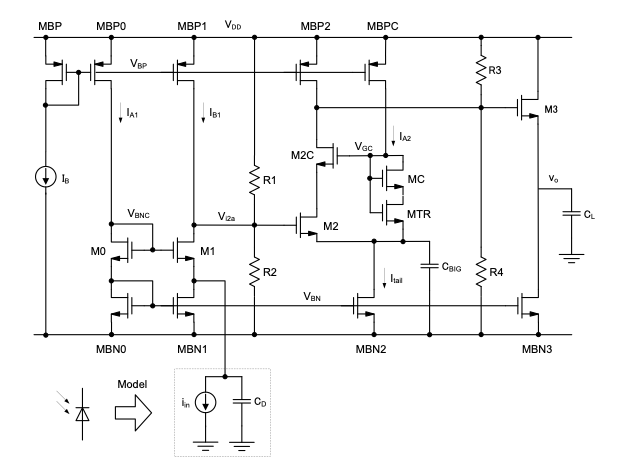
In addition to these above specifications, a major goal of NBE is to create the most robust products on the market. For example, all designers at NBE must refrain from using academically small currents in auxiliary bias nodes. In addition, all current source devices must have at least twice the minimum channel length. Your manager sets the following guidelines for your circuit.
| Parameter | Specification |
|---|---|
| \(I_{A1}/I_{B1}\) | \(\geq 20\%\) |
| \(I_{A1}/I_{\text{tail}}\). | \(\geq 20\%\) |
| \(I_B\) | \(\geq 500 \, \mu A\) |
| \(L_{\text{current\_source}}\) | |
| (applies to MBP, MBP0, MBP1, MBP2, MBPC, | |
| MBN0, MBN1, MBN2, MBN3) | \(\geq 2 \, \mu m\) |
| Triode device width ratio | |
| \((W_{MTR}/W_{MC})\) | \(1/5\) |
| Gate overdrive \((V_{OV})\) for all devices | \(\geq 150 \, mV\) |
You may implement all current mirrors simply by sizing their width ratios. There is no need to work with unit devices (unless you would like to practice doing that). Also, for simplicity in this short project, you are not required to verify the design across PVT variations. In practice, this would be the next logical step after getting your “nominal” design to work. Your manager suggests the following design flow:
◆ Familiarize yourself with the schematic in Figure 6.32 and try to identify key blocks. Review how the bias point of the circuit is established. Draw a simplified half-circuit model that will allow you to identify the “main knobs” in the design.
◆ Setup a design script that allows you to optimize your design iteratively. Identify the key variables that you will focus on; calculate important time constants based on reasonable design choices.
◆ Simulate your design and compare the results to your calculations. Inspect and track down discrepancies. Verify the circuit in a transient simulation using the given input amplitude. A practical hint: The first design you simulate does not have to and probably should not look exactly like the circuit in Figure 6.32. For instance, there is no need to implement all the biasing branches in the very beginning. Start by using ideal current sources for biasing, ideal voltage sources to setup cascodes, etc. Once your idealized design works, it is fairly easy to translate it into the final version that complies with all the constraints (of course, additional parasitics may factor in).
◆ Compile a project report for your boss containing the sections outlined below.
Outline of your design. How did you approach this problem? What are some of your key design choices?
Schematic diagram of final design, with component values, node voltages, and bias currents clearly labeled. Show component values right next to the components, and currents next to the branches. Annotate all transistors with their gate overdrive \(V_{OV}\) (from simulation).
Calculation of key design parameters, such as transconductances, bias currents, etc. This is the most important section of your report. Compare the most relevant hand calculated values with final simulation values in a table and discuss discrepancies.
Simulated bode plot of \(R_m(j\omega)\), phase, and magnitude. Clearly annotate the achieved bandwidth, and transresistance. Annotate your hand calculated values in the same plot.
Show a transient simulation plot of \(v_O\). Set the input amplitude and frequency to 10 μA and 1 MHz, respectively. Show two periods of the waveform and annotate expected quiescent points and peak voltages using horizontal marker lines.
Comments and Conclusion. Here, you can convey issues you may have had, or things you’ve learned/not learned in this project.
Appendix: Final circuit netlist or circuit diagram and operating point output from the simulator.