
1 Introduction
With the development of the integrated circuit, the semiconductor industry is undoubtedly the most influential industry to appear in our society. Its impact on almost every person in the world exceeds that of any other industry since the beginning of the Industrial Revolution. The reasons for its success are as follows:
Exponential growth of the number of functions on a single integrated circuit.
Exponential reduction in the cost per function.
Exponential growth in sales (economic importance) for approximately forty years.
This growth has led to ever-increasing performance at lower prices for consumer electronics such as cellular phones, personal computers, audio players, etc. The computational power available to the individual has increased to the point that it has changed the way we think about problem solving. Communication technology including wired and wireless networks have fundamentally changed the way we live and communicate.
The innovation responsible for these impressive results is the integration of electronic circuit components fabricated in silicon integrated circuit (IC) technology. Today, many of the ICs shaping new applications contain both analog and digital circuitry, and are therefore called mixed-signal integrated circuits. In mixed-signal ICs, the analog circuitry is typically responsible for interfacing with physical signals, and concerned for example with the amplification of a weak signal from an antenna, or driving a sound signal into a loudspeaker. On the other hand, digital circuitry is primarily used for computing, enabling powerful functions such as Fast Fourier Transforms or floating point multiplication.
This module was written as an introduction to the analysis and design of analog integrated circuits in complementary metal-oxide-semiconductor (CMOS) technology. In this first chapter, we will motivate this subject by looking at an example of a mixed-signal IC and by highlighting the need for a systematic study of the fundamental principles and proper engineering approximations in analog design.
Chapter Objectives
Provide a motivation for the study of elementary analog integrated circuits.
Provide a roadmap for the subjects that will be covered throughout this module.
Review fundamental concepts for the construction of two-port circuit models.
1.1 Mixed-Signal Integrated Circuits
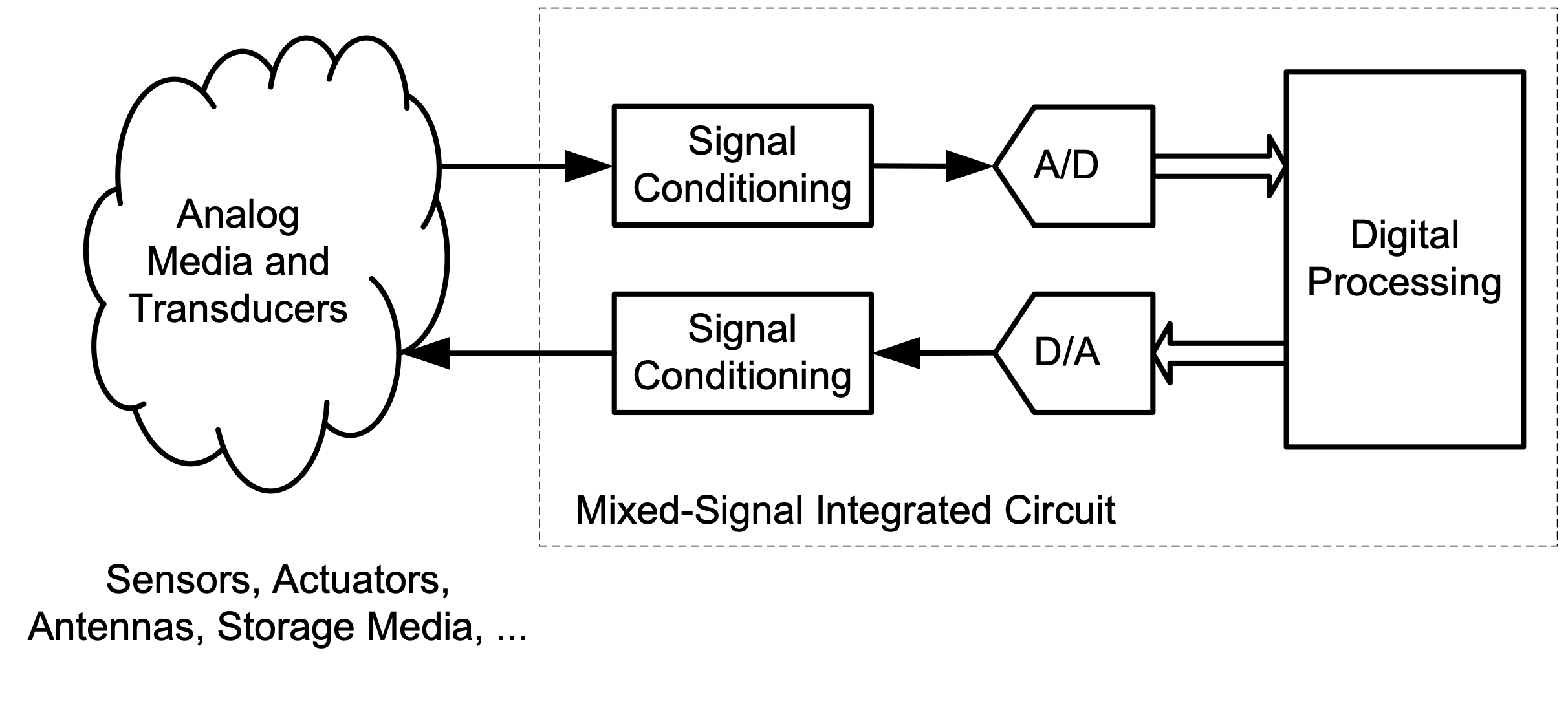
Figure 1.1 shows a generic diagram of a mixed-signal system, incorporating a mixed-signal integrated circuit. To the left of this diagram are the transducers and media that represent the sources and sinks of the information processed by the system. Examples of input transducers include microphones or photodiodes used to receive communication signals from an optical fiber. Likewise, the output of the system may drive an antenna for radio-frequency communication or a mechanical actuator that controls the zoom of a digital camera. At the boundary between the media and transducers are typically signal conditioning circuits that translate the incoming and outgoing signals to the proper signal strength and physical format. For instance, an amplifier is usually needed to increase the strength of the receive signal from a radio antenna, so that it can be more easily processed by the subsequent system components. In most systems, the signal conditioning circuitry interfaces to analog-to-digital and digital-to-analog converters, which provide the link between analog quantities and their digital representation in the computing back-end of the system.
1.1.1 Example: Single-Chip Radio
The block diagram of a modern mixed-signal integrated circuit is shown in Figure 1.2. This design incorporates most of the circuitry needed to realize a modern cellular phone. For instance, it contains a front-end low-noise amplifier (LNA) to condition the incoming antenna signal. The amplified signal is subsequently frequency shifted, converted into digital format and fed into a digital processor. Even though the block diagram in Figure 1.2 looks quite complex, all of its elements can be mapped into one of the blocks of the generic diagram of Figure 1.1.
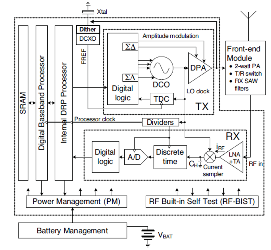
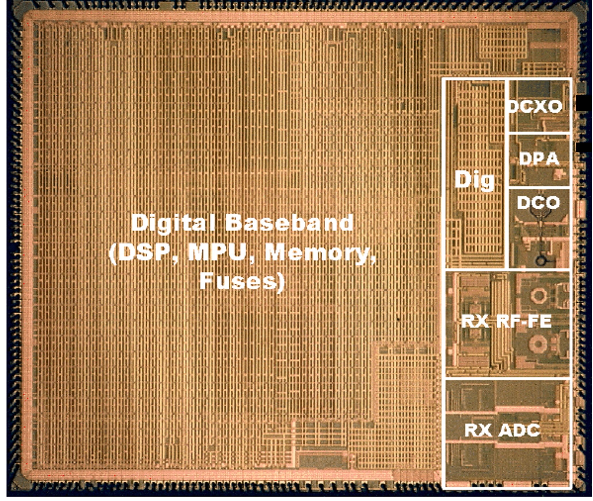
Figure 1.3 shows the chip photo of the single-chip radio, with some of the system’s key building blocks annotated. As evident from this diagram, the digital logic dominates the area of this particular IC. This situation is not uncommon in modern mixed-signal ICs, not least because the utilized digital algorithms have reached an enormous complexity, requiring millions or tens of millions of logic gates.
Staszewski, Robert Bogdan, Dirk Leipold, O Eliezer, Mitch Entezari, Khurram Muhammad, Imran Bashir, C-M Hung, et al. 2008. “A 24mm 2 Quad-Band Single-Chip GSM Radio with Transmitter Calibration in 90nm Digital CMOS.” In 2008 IEEE International Solid-State Circuits Conference-Digest of Technical Papers, 208–607. IEEE.
Despite the dominance of digital logic within most systems, the analog interface components are equally important, as they determine how and how much information can be communicated between the physical world and the digital processing backbone. In many cases, the performance of the signal conditioning and data conversion circuitry ultimately determines the performance of the overall system.
1.1.2 Example: Photodiode Interface Circuit
Figure 1.4 shows an example of a signal conditioning circuit that plays a critical role in fiber-optic communication systems. In such a system, a photodiode is used to convert light intensity to electrical current (\(i_{IN}\)). In order to condition the signal for further processing, the diode current is converted into a voltage (\(v_{OUT}\)) by a so-called transimpedance amplifier. This amplifier must be fast enough to process the incoming light pulses, which often occur at frequencies of multiple gigahertz. In addition, the amplifier must obey certain limits on power dissipation, or the system may become impractical in terms of heat management or power supply requirements.

Limitations in speed and power dissipation are, in general, among the main concerns in the interface circuitry of mixed-signal systems. Since new products tend to demand higher performance, the analog designer is constantly concerned with the design and optimization of system-critical building blocks, aiming for the best possible performance that can be achieved within the framework of the target application and process technology.
A specific example for the circuit realization of a transimpedance amplifier is shown in Figure 1.5. It consists of three transistor stages, each of which serves a specific purpose and design intent. This is true for most amplifier circuits; even though the full schematic of a particular realization may be com- plex, it can usually be broken up into smaller sub-blocks that are more easily understood. Specifi- cally, for the amplifier of Figure 1.5, the experienced designer will recognize that the circuit consists of a cascade connection of a common-gate, common-source, and common-drain stage. These sub-blocks form the basis for a large number of analog circuits, and can be viewed as the “atoms” or fundamental building blocks of analog design. In this module, you will learn to analyze these blocks from first principles, and to reuse the gained knowledge for the design of more complex circuits. The circuit of Figure 1.5 will be analyzed in detail in Chapter 6 of this module, building upon the principles covered in Chapters 2–5.
1.2 Managing Complexity
As evident from the example of Section 1-1-1, modern integrated circuits are highly complex and require a hierarchical approach in design and analysis. That is, a modern integrated circuit is far too complex to be fully understood and analyzed in a single sheet schematic at the transistor level. Typically, a mixed-signal IC is represented by a block diagram as the one shown in Figure 1.2. At the level of this description, suitable specifications are derived for each block, which may itself contain several sub-blocks. The blocks and sub-blocks are then designed and optimized until they meet the desired target specifications.

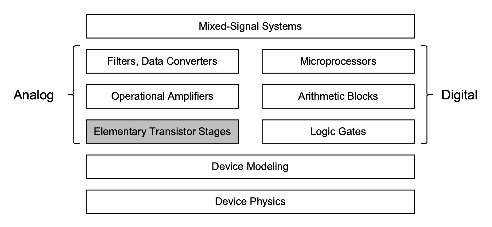
Figure 1.6 illustrates examples of the various levels of abstraction that come into play in the design of a modern integrated circuit. At the highest level, the constituent elements can be partitioned into analog and digital blocks. An example of a high-level analog block is an analog-to-digital converter, whereas a microprocessor is an example of a large digital block. These blocks themselves contain smaller functional units, as, for example, operational amplifiers in the case of an analog-to-digital converter. The operational amplifiers themselves contain the aforementioned elementary transistor stages, which are the main subject of this module.
Interestingly, even at the level of elementary transistor stages, is often not possible to work with a perfect model or description of the circuit. This is particularly so because the physical effects in the constituent transistors are highly complex and often impossible to capture perfectly with a tractable set of equations for hand analysis. Therefore, making proper engineering approximations in transistor modeling is an important aspect in maintaining a systematic design methodology. For this particular reason, the presentation in this module follows a “just-in-time” approach for the modeling of transistor behavior. Rather than deriving a complete transistor model in an isolated chapter (as done in most texts), we begin with only the basic device properties and increase complexity throughout the module upon demand, and where needed to gain further insight and accuracy. With this approach, the reader learns to appreciate the complexity of a refined model, and will be able to assess and track potential limitations of working with simplified models.

1.3 Two-Port Abstraction for Amplifiers
High-level system block diagrams, such as Figure 1.2 , are typically drawn as unidirectional flowcharts and do not capture details about the electrical behavior of each connection port and how certain blocks may interact once they are connected. Unfortunately, electrical signals are not unidirectional, and connecting two blocks always means that there is some level of interaction through the voltages and currents at the connection points.
The commonly used linear two-port modeling abstraction for amplifiers and amplifier stages allows the designer to take these effects into account while maintaining a high level of abstraction. For instance, the circuit of Figure 1.5 can be approximately modeled as shown in Figure 1.7 (the details on obtaining this model are discussed later in this module). Each stage of the overall amplifier is represented via a simplified circuit model that captures its essential features. Once this model is created, the interaction among stages can be analyzed at this high level of abstraction, without requiring detailed insight on how each stage is implemented. The two-port modeling approach is particularly useful in the design of amplifiers, as it can help shape the thought process on how the various stages should be configured to optimize performance. In the following subsections, we will review some of the basic concepts of amplifier two-port modeling used in this module.
1.3.1 Amplifier Types
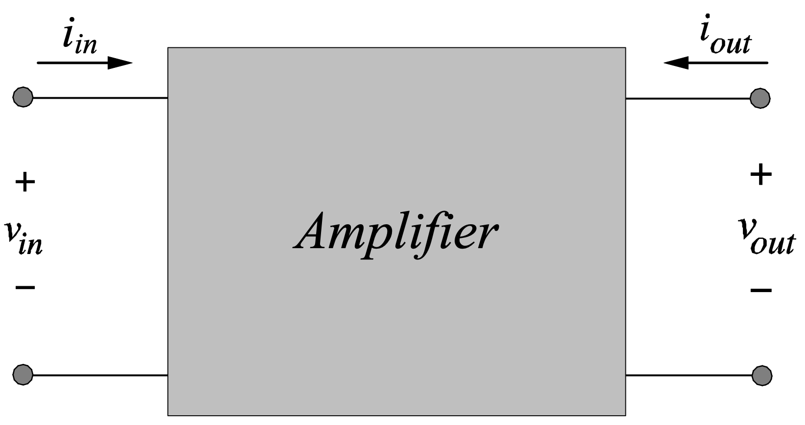
In this module, we model amplifier circuits as blocks that have an input and output port, where the term “port” refers to a pair of terminals. For each port, we can define input and output currents and voltages as shown in Figure 1.8. Depending on the intended function, we distinguish between the four possible amplifier types listed in Table 1-1. For example, an amplifier that takes an input current and amplifies this current to produce a proportional output voltage is called a transresistance amplifier. In this context, it is important to emphasize that in a general practical amplifier circuit, the input and output ports will always carry both nonzero voltages and currents, and there exist transfer functions between all possible combinations of input/output variables. What truly defines the type of an amplifier is what the circuit designer deems as the main quantities of interest in the amplifier’s application.
| Amplfier Type | Input Quantity | Output Quantity |
|---|---|---|
| Voltage Amplifier | Voltage | Voltage |
| Current Amplifier | Current | Current |
| Transconductance Amplifier | Voltage | Current |
| Transresistance Amplifier | Current | Voltage |
Now, in order to model the inner workings of each amplifier type, we can invoke the four corresponding two-port amplifier models shown in Figure 1.9. Each amplifier model has an input and output resistance (or more generally, a frequency dependent impedance) and a controlled source to model the amplification.
In the voltage amplifier model, the controlled source is a voltage-controlled voltage source. Ideally, the input resistance is infinite (open circuit, no current flow). The ideal output resistance is zero (ideal voltage source).
The current amplifier model has a current-controlled current source. Ideally, the input resistance is zero (short circuit, no voltage across the input port) and the output resistance is infinite (ideal current source).
The transconductance amplifier model has a voltage-controlled current source. Ideally, the input resistance is infinite (open circuit, no current flow). The ideal output resistance is also infinite (ideal current source).
The transresistance or transimpedance1 amplifier model has a current-controlled voltage source. Ideally, the input resistance is zero (short circuit, no voltage across the input port). The ideal output resistance is also zero (ideal voltage source).
1 The term transimpedance is sometimes used to refer to an amplifier that is primarily meant to realize a transresistance. Referring to “impedance” highlights the fact that the transfer function will usually be frequency-dependent.
From these four models and their ideal behavior, we note that the two-ports containing a voltage-controlled source should ideally have large input resistance (\(R_{in}\)). This minimizes the signal loss due to resistive voltage division between the source voltage (\(v_s\)) and the control voltage (\(v_{in}\)). In contrast, the two-ports that use a current-controlled source should have small input resistance to minimize the signal loss due to current division between the source current (\(i_s\)) and the control current (\(i_{in}\)). In this context, “large” and “small” refer to the value of \(R_{in}\) relative to the source resistance (\(R_s\)).
On the output side, if the variable of interest is a voltage, the output resistance (\(R_{out}\)) should be small so that only a small amount of the amplified voltage is lost through the division with the load (\(R_L\)). Conversely, for a current output, the output resistance should be large to minimize current division losses. Again, “large” and “small” are taken as relative measures comparing Rout to \(R_L\).
Consider for example the voltage amplifier of Figure 1.9(a). To calculate the transfer function of the overall circuit (\(v_{out}\)/\(v_s\)), the input voltage, including its source resistance, is connected to the input of the two-port model and the load resistance is connected to the output. The full circuit is shown in Figure 1.10.
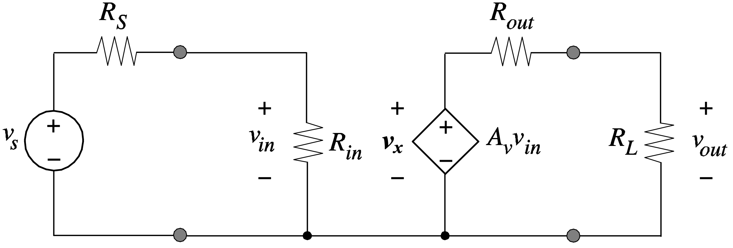
Applying the voltage divider rule at the input and output of the circuit gives
\[ \frac{v_{out}}{v_s} = \Bigl(\frac{v_{in}}{v_s}\Bigr) \cdot A_v \cdot \Bigl(\frac{v_{out}}{v_x}\Bigr) = \Bigl(\frac{R_{in}}{R_{in} + R_s}\Bigr) \cdot A_v \cdot \Bigl(\frac{R_{L}}{R_{L} + R_{out}}\Bigr) \tag{1.1}\]
As we can see from this expression, the overall voltage gain is maximized when the amplifier has a large input resistance (relative to \(R_s\)) and a small output resistance (relative to \(R_L\)). For the ideal case of infinite input resistance and zero output resistance, \(v_{out}\)/\(v_s\) becomes equal to \(A_v\).
For the sake of compact notation, we will often want to use a symbol for the overall circuit gain. The notation used in this module uses primed variables to distinguish between the gain of the controlled source and the gain of the overall amplifier circuit. For example, for the above-discussed voltage amplifier we define \(A'_v\) = \(v_{out}\) ⁄ \(v_s\). This notation is meant to emphasize the connection between the two symbols. \(A'_v\) is usually smaller than \(A_v\), but can approach \(A_v\) for ideal source and load configurations.
Example 1-1: Transfer Function Transconductance Amplifier.
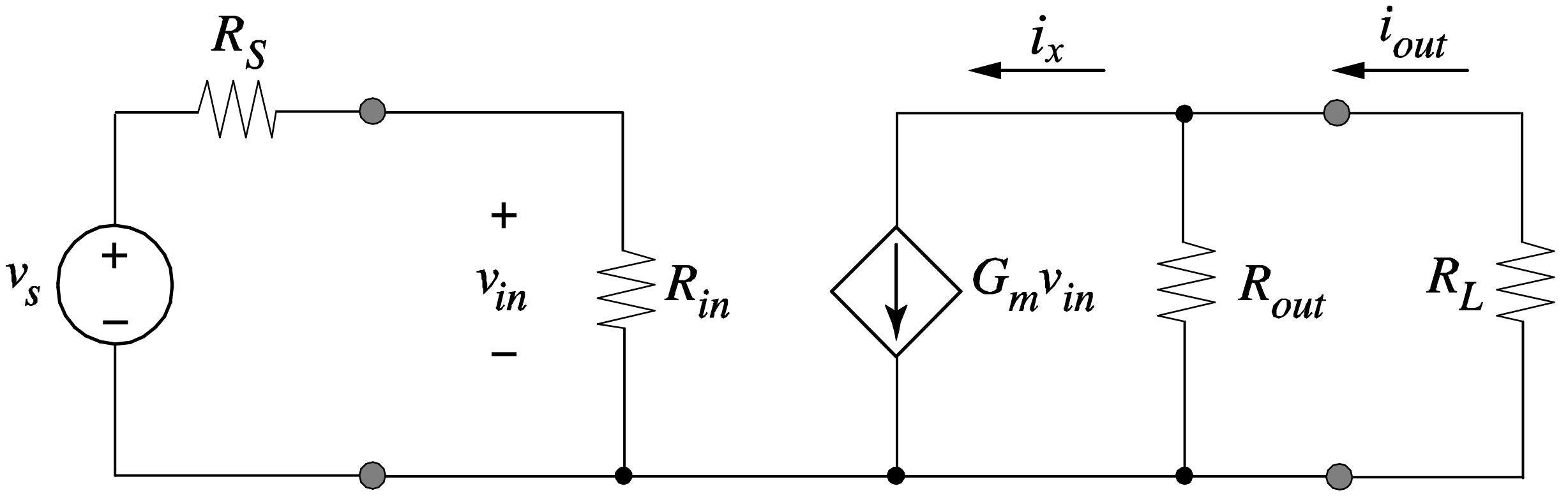
For the transconductance amplifier circuit in Figure 1.11, calculate the overall transconductance \(G'_m = i_{out} ⁄ v_s\).
SOLUTION
Applying the voltage divider rule at the input and the current divider rule at the output yields the following result:
\[ G'_m = \frac{i_{out}}{v_s} = \Bigl(\frac{v_{in}}{v_s}\Bigr) \cdot G_m \cdot \Bigl(\frac{i_{out}}{i_x}\Bigr) = \Bigl(\frac{R_{in}}{R_{in} + R_s}\Bigr) \cdot G_m \cdot \Bigl(\frac{R_{out}}{R_{L} + R_{out}}\Bigr) \]
Thus, the overall transconductance gain is maximized when the amplifier has a large input resistance (relative to \(R_s\)) and a large output resistance (relative to \(R_L\)). For the ideal case of infinite input and output resistances, \(G'_m\) becomes equal to \(G_m\).
As a final remark for this sub-section, it is important to recognize that all of the models in Figure 1.9 can be used interchangeability to describe the exact same electrical behavior (see Problem P1-1). For instance, a voltage amplifier model can be converted into a transconductance amplifier model by applying a Thevénin to Norton transformation for the controlled source.
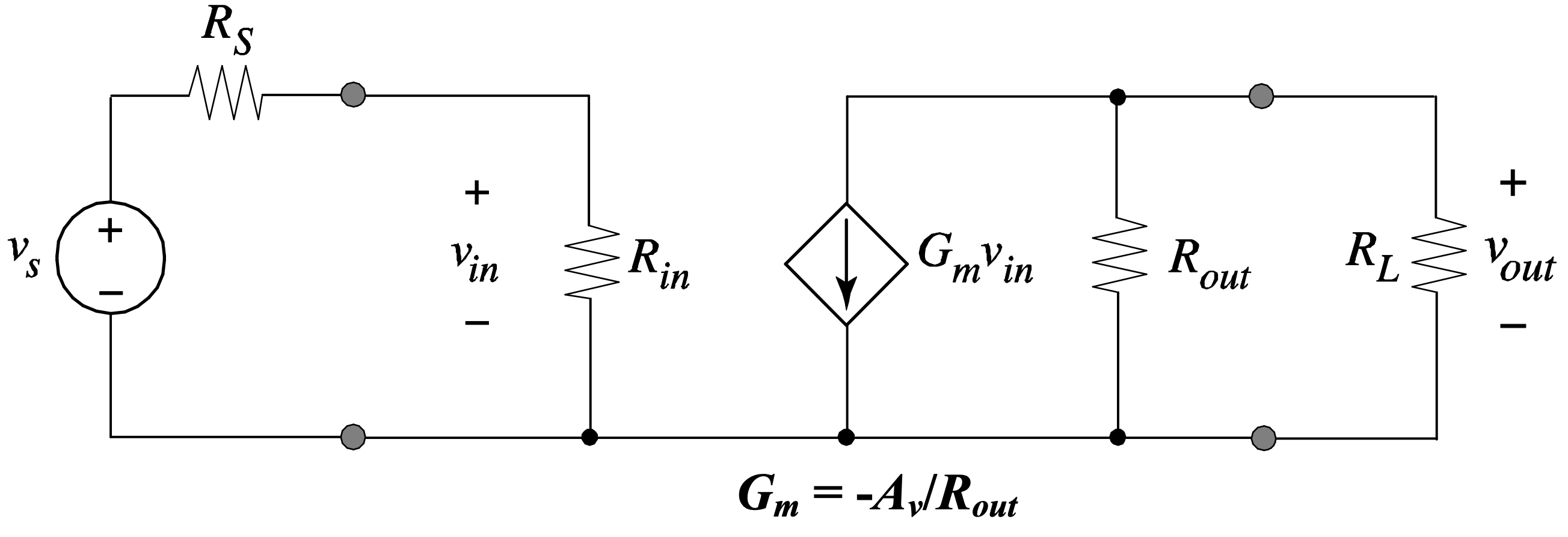
A corollary to this equivalence is that we can for example use a transconductance amplifier model to describe a voltage amplifier circuit. This is illustrated through the circuit of Figure 1.12, which is electrically equivalent to that of Figure 1.10 (see Problem P1-2). Note that the output is taken as the voltage across the output port instead of the output current; this indicates that the circuit is viewed as a voltage amplifier. Just as in the original circuit of Figure 1.10, we require a large input resistance and small output resistance for this circuit to maximize the overall voltage gain.
The choice of amplifier model depends on several factors. At first glance, it seems natural to model each amplifier type using its “native” model that directly corresponds to the intended function. For example, we could always describe a voltage amplifier using the corresponding voltage amplifier model that contains a voltage controlled voltage source. However, as we shall see throughout this module, it is sometimes more convenient to align the amplifier model with the physical amplification mechanism or a structural feature of the underlying transistor circuit. For instance, the common-source voltage amplifier discussed in Chapter 2 naturally invokes a transconductance-based model due to the physical model of the employed transistor.
1.3.2 Unilateral versus Bilateral Two-Ports
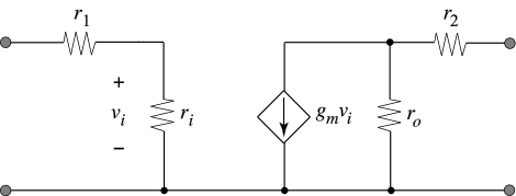
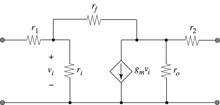
All of the two-port models shown in Figure 1.9 are called unilateral, because they can only propagate a signal from the input port to the output port and not the other way around. For instance, injecting a current into the output port of the current amplifier of Figure 1.9(b) will not induce a current at the input port. Unfortunately, many practical transistor circuits are not unilateral, and exhibit bilateral behavior when analyzed in detail, and especially at high frequencies.
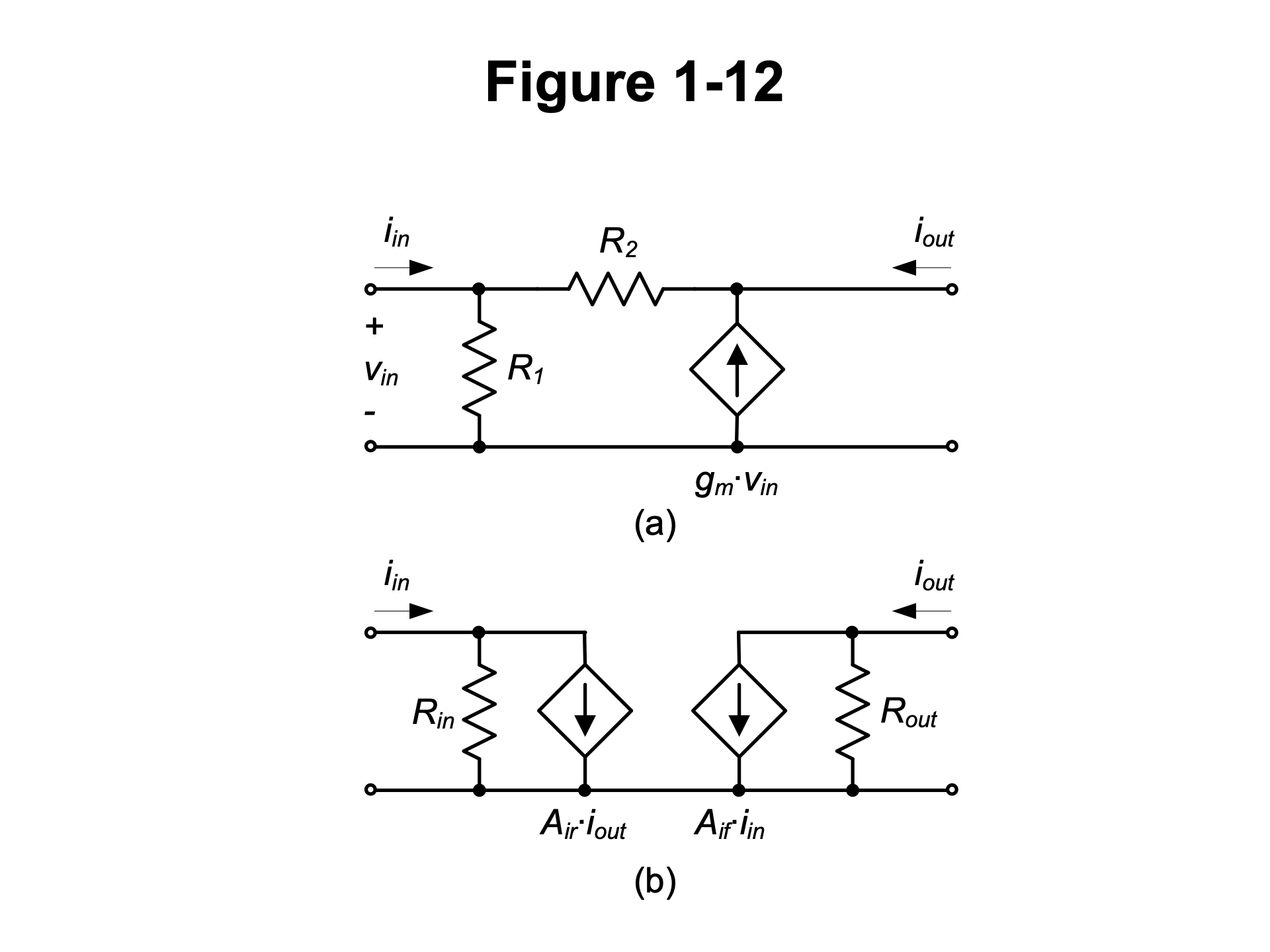
An example of a bilateral current amplifier is shown Figure 1.13(a). Note that in this circuit, resistor \(R_2\) couples the input and output networks and it can therefore transfer currents in both directions. Consequently, the unilateral model of Figure 1.9(b) cannot perfectly represent this circuit. When it is desired to capture the bilateral behavior, the two-port model in Figure 1.13(b) could be employed in principle. Here, the controlled source Air models the reverse current transfer from the output back to the input. Alternatively, one could employ other bilateral and more general two-port models based on admittance parameters (\(Y\)), impedance parameters (\(Z\)), and hybrid or inverse-hybrid parameters (\(H\) or \(G\)); see advanced circuit design texts such as (Gray et al. 2009). These models are particularly useful when reverse transmission (i.e., feedback from the output to the input) is incorporated in the circuit as part of the intended design.
Gray, Paul R, Paul J Hurst, Stephen H Lewis, and Robert G Meyer. 2009. Analysis and Design of Analog Integrated Circuits. John Wiley & Sons.
There are two reasons why we will work exclusively with unilateral two-port approximations in this module. First, the circuits considered are designed primarily to implement forward gain rather than reverse gain; feedback circuits are not treated in this module. For example, referring to the model of Figure 1.13(b), the reverse gain Air will be negligibly small in any current amplifier circuit that we will consider. Second, a clear drawback of working with bilateral two-port models would be a significant increase in analysis complexity. As we have seen in Example 1-1, the overall transfer function of a unilateral two-port circuit can be written by applying simple voltage and current divider rules. This also extends to cascade connections of multiple two-ports. For example, the overall transfer function of the circuit in Figure 1.7 is easily written by inspection, without requiring extensive algebra. With reverse transmission included, the transfer function analysis will generally require solving a linear system of equations. In light of the fact that we do not intend to design circuits in this module that have significant reverse transmission, this increase in complexity is not welcome, and would also hinder us from developing intuition from inspection-driven analysis.
1.3.3 Construction of Unilateral Two-Port Models
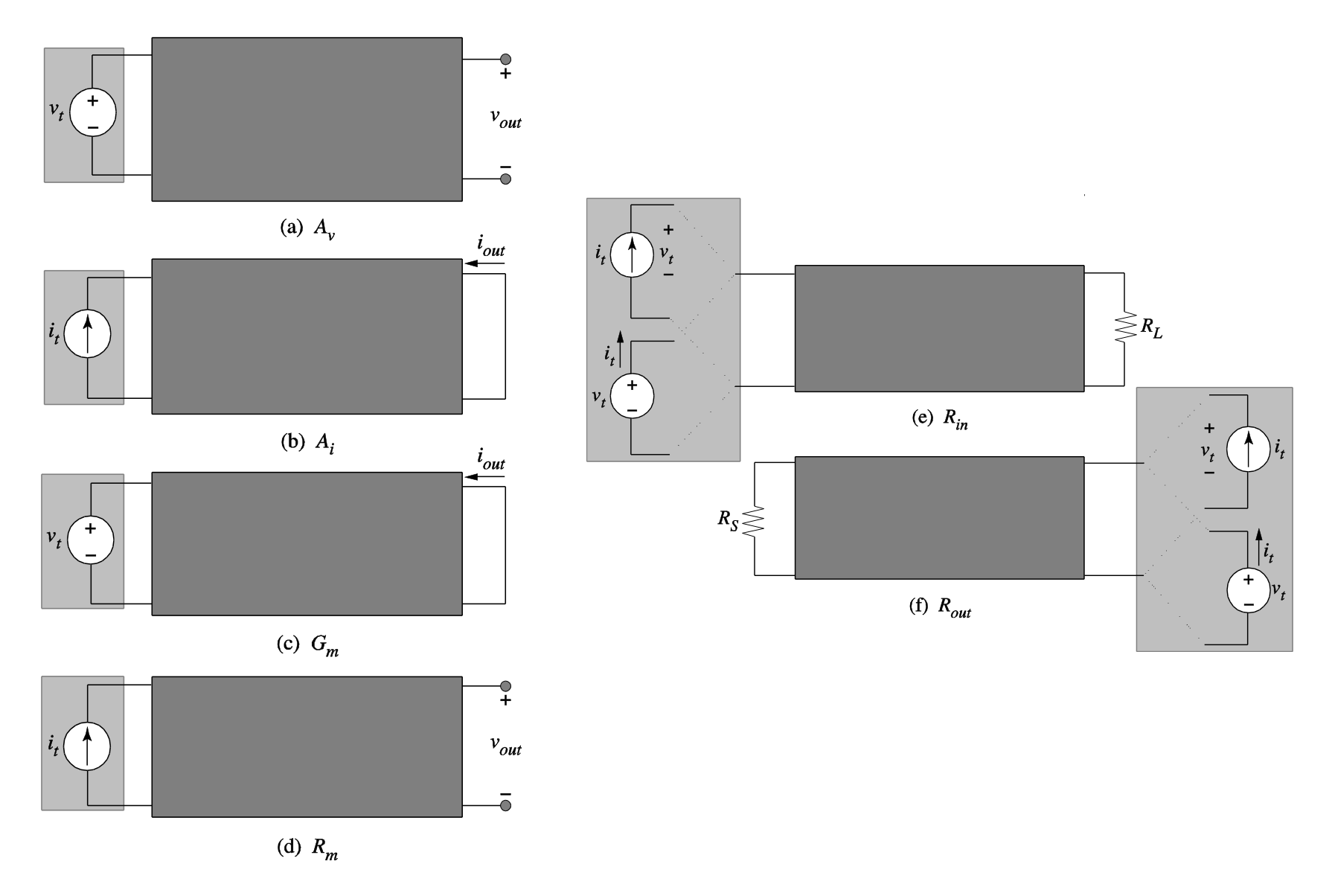
We will now describe the general procedures to calculate the controlled sources, as well as the input and output resistances, for the unilateral two-port models of Figure 1.9. The approach is based on applying test voltages and currents to find the desired model parameters.
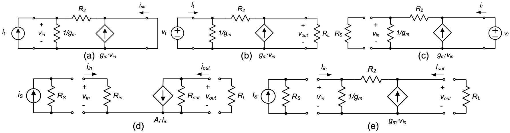
The most important parameter of any amplifier circuit is its gain. To identify the gain parameters for the models of Figure 1.9(a)-(d), we apply the tests shown in Figure 1.14(a)-(d), respectively.
To calculate the gain term \(A_v\) of a voltage amplifier model, we apply a test voltage at the input with zero source resistance and measure the open-circuit output voltage. \(A_v = v_{oc} / v_t\) is therefore also called the open-circuit voltage gain.
To calculate the gain term \(A_i\) of a current amplifier model, we apply a test current at the input with infinite source resistance and measure the short-circuit output current. \(A_i = i_{sc} / i_t\) is therefore also called the short-circuit current gain.
To calculate the gain term \(G_m\) of a transconductance amplifier model, we apply a test voltage at the input with zero source resistance and measure the short-circuit output current to find \(G_m = i_{sc}/v_t\).
To calculate the gain term \(R_m\) of a transresistance amplifier model, we apply a test current at the input with infinite source resistance and measure the open-circuit output voltage to find \(R_m = v_{oc} / v_{it}\).
The rationale behind these tests can be understood by considering, for example, the case of the voltage amplifier model of Figure 1.9(a). When driven with an ideal voltage source, the effect of any resistance at the input port is eliminated, and the controlled source is directly stimulated by the applied test source (without any voltage division). Likewise, by measuring the resulting output voltage open-circuited, any resistance in series with the controlled source has no effect and the measurement therefore accurately extracts the parameter \(A_v\). Similar explanations apply to the test cases for the remaining amplifier models.
The test setup for extracting the input and output resistances for all amplifier models is shown in Figure 1.14(e), and (f), respectively.
To calculate the input resistance \(R_{in}\) we apply a test voltage and measure the current coming from the test source, or apply a test current and mea- sure the voltage across the test source. In this test, the load resistance (\(R_L\)) must be connected to the output port as shown in Figure 1.14(e).
To calculate the output resistance \(R_out\), we apply either a test voltage or a test current source at the output port and measure the respective current or voltage from the source. Here, the input source must be set equal to zero. This means that input voltage sources are shorted and input current sources are open-circuited. Only the source resistance (\(R_S\)) is left across the input terminals as shown in Figure 1.14(f).
The above procedures extract the input and output resistances perfectly and without any approximations, even if the circuit is bilateral. As we shall see through the examples below, \(R_{in}\) and \(R_{out}\) do not depend on \(R_L\) and \(R_S\), respectively, in a perfectly unilateral amplifier. However, this is not the case in a bilateral amplifier, and therefore the general procedure includes \(R_L\) and \(R_S\) in the test setup.
In summary, the above procedures for measuring unilateral two-port model parameters aim at finding the best possible unilateral representation of an arbitrary amplifier circuit, which itself may or may not be unilateral. The obtained models are approximate when the amplifier is bilateral, since they do not include a controlled source that captures reverse transmission from the output back to the input. In most cases considered in this module, the reverse transmission term is negligible. Exceptions will be highlighted and treated as appropriate.
Example 1-2: Two-Port Model Calculations for a Unilateral Amplifier
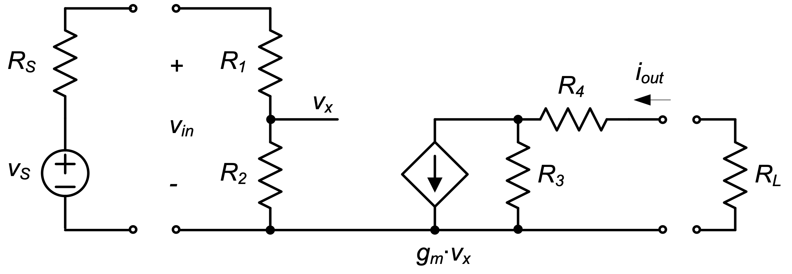
For the transconductance amplifier in Figure 1.15, calculate the following two-port model parameters: the transconductance \(G_m\), the input resistance \(R_{in}\), and the output resistance \(R_{out}\). Also, compute the overall transfer function \(G'_m = i_{out} ⁄ v_s\).
SOLUTION
To find the transconductance, we short the output port and apply an ideal test voltage source (\(v_t\)) at the input (see Figure 1.15). From this circuit, we see that
\[ G_m = \frac{i_{sc}}{v_t} = \frac{g_m v_x \cdot \frac{R_3}{R_3 + R_4}}{v_t} = \frac{g_m v_x \cdot \frac{R_2}{R_1 + R_2} \cdot \frac{R_3}{R_3 + R_4}}{v_t} = g_m \cdot \frac{R_2}{R_1 + R_2} \cdot \frac{R_3}{R_3 + R_4} \]
Next, to find \(R_in\), we apply a test voltage at the input and connect the load resistance \(R_L\) at the output (Figure 1.16). From this circuit, we find that the input resistance is simply the series connection of \(R_1\) and \(R_2\), i.e., \(R_{in} = R_1 + R_2\). Note that the output network does not influence this result.
Finally, to find \(R_{out}\), we apply a test voltage at the output and connect the source resistance \(R_S\) across the input port (the source \(v_s\) is replaced by a short), (see Figure 1.16(c)). In the resulting circuit, \(v_x\) must be zero, because no current is flowing in the input network. Thus, the controlled source carries no current and we conclude that \(R_{out} = R_3 + R_4\).
In order to compute the transfer function of the complete circuit, we can reuse the result obtained in Example 1-1.
\[ G'_m = \frac{i_{out}}{v_s} = \Bigl(\frac{R_{in}}{R_{in} + R_s}\Bigr) \cdot G_m \cdot \Bigl(\frac{R_{L}}{R_{L} + R_{out}}\Bigr) \]
Substituting \(G_m\), \(R_{in}\), and \(R_{out}\) from the above calculation yields the final result.
\[ G'_m = \frac{i_{out}}{v_s} = \frac{g_m R_2 R_3}{(R_1 + R_2 + R_S)(R_L + R_3 + R_4)} \]
In the preceding example, we have seen that the source and load resistances have no effect on the extracted two-port parameters. In the following example, we will investigate a bilateral circuit to show that in general, the input and output resistances depend on \(R_S\) and \(R_L\), which must therefore always be included in the general two-port modeling calculations.
Example 1-3: Two-Port Model Calculations for a Bilateral Amplifier
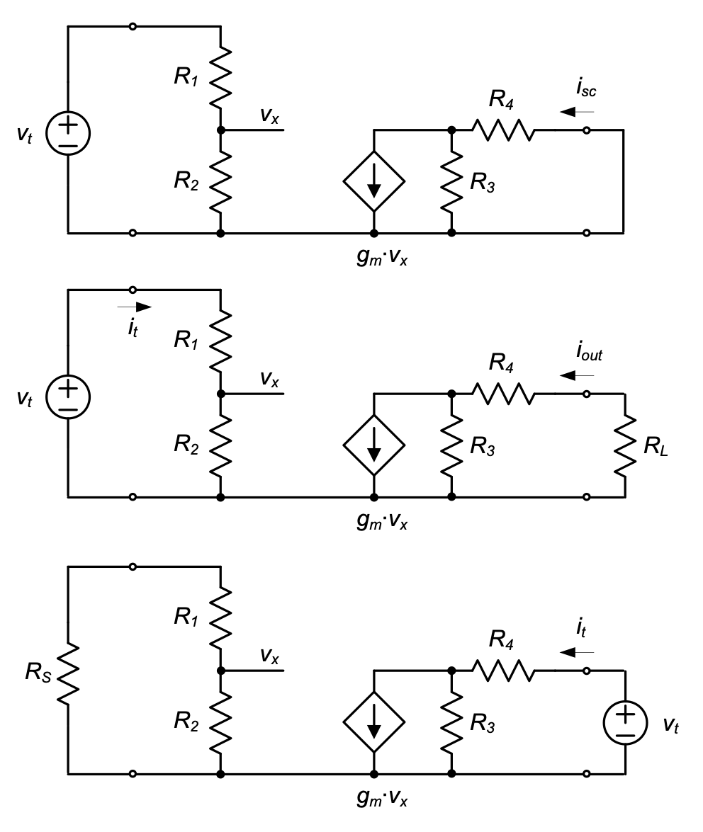
For the current amplifier in Figure 1.13(a), calculate the following unilateral two-port model parameters: the current gain \(A_i\), the input resistance \(R_{in}\), and the output resistance \(R_{out}\). Also, compute the overall transfer function \(i_{out} / v_s\) using the obtained unilateral two-port model. Compare the result to a direct KCL-based analysis of the transfer function. Assume that the circuit is driven by a current source with resistance \(R_S\) and loaded by a resistance \(R_L\). For algebraic simplicity, assume \(R_1 = 1 / g_m\) (this case corresponds to the common-gate amplifier circuit covered in Chapter 4).
SOLUTION
To find the current gain Ai, we short the output port and apply an ideal test current source (\(i_t\)) at the input (see Figure 1.17(a)). From this circuit, we see that
\[ v_{in} = \Bigl( g_m + \frac{1}{R_2} \Bigr)^{-1} \cdot i_t \]
and
\[ i_{sc} = - \Bigl( g_m + \frac{1}{R_2} \Bigr) \cdot v_{in} \]
Thus, Ai = isc/it = –1.
Next, to find \(R_{in}\), we apply a test voltage at the input and connect the load resistance \(R_L\) at the output (Figure 1.17(b)). From this circuit, we note that the input resistance is not easily identified by inspection. Hence we write KCL for the two nodes of the circuit (\(v_t\) and \(v_out\)).
\[ 0 = -i_t + g_m v_t + \frac{v_t - v_out}{R_2} \]
\[ 0 = - g_m v_t + \frac{v_{out}}{R_L} + \frac{v_t - v_out}{R_2} \]
Solving this system of equations yields
\[ R_{in} = \frac{v_t}{i_t} = \frac{R_2 + R_L}{1 + g_m R_2} = \frac{1 + \frac{R_L}{R_2}}{g_m + \frac{1}{R_2}} \]
Note from this result that \(R_in\) depends on \(R_L\), as mentioned previously; this dependency stems from the bilateral structure of the circuit. Also note that Rin approaches \(1 / g_m\) when \(R_2\) is large compared to \(R_L\) and $ 1 / g_m$. We will revisit this important point in Chapter 4, in the context of a common-gate amplifier circuit.
Now, to find \(R_{out}\), we apply a test voltage at the output and connect the source resistance \(R_S\) across the input port Figure 1.17. Again, we must write KCL at the two circuit nodes and solve the resulting system of equations. This yields
\[ R_{out} = \frac{v_t}{i_t} = R_2 R_S + g_m R_2 R_S \]
Again, note that \(R_out\) is a function of \(R_S\); this is the case for any bilateral circuit.
Finally, to compute the transfer function based on the obtained unilateral model, we consider the circuit shown in Figure 1.17(d). By inspection, we see that
\[ A_i' \frac{i_{out}}{i_s} = \Bigl( \frac{R_S}{R_{in} + R_S} \Bigr) A_i \frac{R_{out}}{R_L + R_{out}} \]
Substituting \(A_i\), \(R_{in}\), and \(R_{out}\) from the above calculation into this expression yields
\[ A_{i, Two-Port}' = \frac{i_{out}}{i_s} = -\frac{R_S(1 + g_m R_2)(R_2 + R_S + g_m R_2 R_S)}{(R_L + R_2 + R_S + g_m R_2 R_S)^2} \]
We now wish to compare this result to the accurate transfer function of the circuit, obtained by direct calculation and without approximating the circuit as a unilateral two-port. For this purpose, we consider the full circuit shown in Figure 1.17(e) and write KCL for its two nodes.
\[ 0 = - i_s + g_m v_in + \frac{v_{in}}{R_S} + \frac{v_{in} - v_{out}}{R_2} \]
\[ 0 = -g_m v_{in} + \frac{v_{out}}{R_L} + \frac{v_{out} - v_{in}}{R_2} \]
Solving this system of equations for \(v_{out}\) and substituting \(i_{out} = - v_{out} / R_L\) yields
\[ A_{i, Exact}' = \frac{i_{out}}{i_s} = -\frac{R_S (1 + g_m R_2)}{R_L + R_2 + R_S + g_m R_2 R_S} \]
The discrepancy factor between the two results is given by
\[ \frac{A_{i, Two-Port}'}{A_{i, Exact}'} = \frac{R_2 + R_S + g_m R_2 R_S}{R_L + R_2 + R_S + g_m R_2 R_S} = \frac{1 + R_S \Bigl(\frac{1}{R_2} + g_m \Bigr)}{1 + \frac{R_L}{R_2} + R_S \Bigl(\frac{1}{R_2} + g_m \Bigr)} \]
From this result, we see that the discrepancy factor approaches unity (no error) when \(R_2\) is much larger than \(R_L\), a condition that is often satisfied in practice (the ideal load for a current amplifier is a short circuit). In this case, the unilateral two-port model will accurately describe the behavior of the circuit.
The outcome of the above example captures the main spirit in which we justify relying on unilateral two-port models in this module. Even though the considered amplifier is strictly speaking bilateral, a unilateral model describes its behavior to within the desired engineering accuracy, provided that reason- able boundary conditions hold.
1.4 Integrated Circuit Design versus Printed Circuit Board Design
In the design of analog circuits, the underlying technology has a significant impact on the choice of architecture, because it tends to restrict the availability and specification range of the underlying active and passive components. For instance, a designer working with discrete components on a printed circuit board may be subjected to the following constraints:
Limit the component count below 100 elements to achieve a small board area.
Resistors can be chosen in the range of 1Ω–10MΩ.
Capacitors can be chosen in the range of 1pF–10,000 μF.
The resistor and capacitor values match to within 1–10%.
The available (discrete) bipolar junction transistors match to within 20% in their critical parameters.
In contrast, the designer of a CMOS system-on-chip may face the constraints summarized below:
Avoid using resistors; use as many MOSFET transistors as needed (within reasonable limits, on the order of hundreds to several thousands) to realize the best possible circuit implementation.
Capacitors can be chosen in the range of 10 fF–100 pF.
The critical parameters in the MOSFET transistors be made to match to within 1%, but vary by more than 30% for different fabrication runs.
Capacitors of similar size can match to within 0.1%, but vary by more than 10% for different fabrication runs.
As a consequence of the vastly different constraints that apply to the design of analog circuits in CMOS technology, the resulting practical and preferred circuit architectures differ substantially from the ones that would be used in a printed circuit board design. For example, a discrete voltage amplifier may utilize large AC coupling capacitors to simplify and decouple the biasing of the individual gain stages (see example in Figure 1.18). In contrast, it is typically not possible to use AC coupling techniques (except for very high-frequency designs) in integrated circuits, primarily due to the restriction on maximum capacitor size.
The material covered in this module is primarily concerned with analog integrated circuit design. While this choice does not affect many of the key principles used in the analysis and the discussed circuits, it does affect the architectural choices made in arriving at a practical design. For instance, large AC coupling capacitors are not used throughout the discussion. Also, where appropriate, we will invoke certain assumptions about the typical matching of component parameters in CMOS to eliminate impractical design choices.
1.5 Prerequisites and Advanced Material
The reader of this module is expected to be familiar with the basis concepts of linear circuit analysis (see Ulaby and Maharbiz 2013), including
Ulaby, Fawwaz Tayssir, and Michel M Maharbiz. 2013. Circuit Analysis and Design. 2nd Edition. NTS Press.
Passive components (resistors, capacitors)
Kirchhoff’s voltage and current laws (KVL and KCL)
Independent and dependent voltage and current sources; Thevénin and Norton representation of controlled sources
Two-port representation of circuits; calculation of port resistances and frequency dependent impedances
Manipulation of complex variables and numbers
Phasor analysis and Laplace domain representation of passive circuit elements
Bode plots
The derivations of device models in this module assume familiarity with basic solid-state physics and electrostatics as treated in introductory texts on solid-state device physics (see Pierret 1996). A few sections of this module are marked with an asterisk (*) to indicate advanced material that may in some cases go beyond the learning goals of an introductory course. These sections can be skipped at the instructor’s discretion without affecting the overall flow and context.
Pierret, R. F. 1996. Semiconductor Device Fundamentals. Pearson Education. https://books.google.com/books?id=P-VNFYbs3r0C.
1.6 Notation
This module follows the notation for signal variables as standardized by the IEEE. Total signals are composed of the sum of DC quantities and small signals. For example, a total input voltage \(v_{IN}\) is the sum of a DC input voltage \(V_{IN}\) and a small-signal voltage \(v_{in}\). The notation is summarized below.
Total quantity has a lowercase variable name and uppercase subscript
DC quantity has an uppercase variable name and uppercase subscript
Small-signal quantity has a lowercase variable name and lowercase subscript
1.7 Summary
This chapter offered a brief motivation for the topics covered in this module, which focuses on the analysis and design of elementary amplifier stages in CMOS technology. These elementary stages can be viewed as the “atoms” of analog circuit design and a thorough understanding of the blocks is a necessary prerequisite for the design of advanced analog circuits design, as for instance in the context of large systems-on-chip. At all levels of circuit design, complexity is managed using hierarchical abstraction and model simplification using proper engineering approximations. The unilateral two-port models reviewed in Section 1-3 and used throughout this module, are an example of such abstractions.
1.8 Problems
P1.1 Given the amplifier circuit in Figure 1.19 (a) Find the input and output resistance. (b) Construct an equivalent circuit using a voltage amplifier two-port model and determine all model parameters symbolically. (c) Repeat part (b) for a current amplifier model. (d) Repeat part (b) for a transconductance amplifier model. (e) Repeat part (b) for a transresistance amplifier model.
P1.2 Convince yourself that the circuits of Figure 1.10 and Figure 1.12 are equivalent by showing sym- bolically that both circuits have the same overall voltage gain \(A'_v = v_{out} ⁄ v_s\).
P1.3 You are given an input voltage source with a source resistance, \(R_S\). (a) Use the unilateral voltage amplifier two-port model found in P1.1 to find the overall voltage gain when the amplifier is driving a load resistor \(R_L\). (b) Specify whether the resistances \(r_1\), \(r_i\), \(r_o\), \(r_2\) in the small signal model should be increased, be decreased, or remain the same to improve the overall voltage gain.
P1.4 You are given an input current source with a source resistance, \(R_S\). (a) Use the unilateral current amplifier two-port model found in P1.1 to find the overall current gain when the amplifier is driving a load resistor \(R_L\). (b) Specify whether the resistances \(r_1\), \(r_i\), \(r_o\), \(r_2\) in the small-signal model should be increased, be decreased, or remain the same to improve the overall current gain.
P1.5 Given the circuit model in Figure 1.20 for an amplifier circuit (with \(r_i\) and \(r_o\) removed and \(r_1\)=\(r_2\)=0)
- Find the input and output resistance. Note that since this circuit is bilateral, \(R_S\) must be considered when computing \(R_{out}\), and \(R_L\) must be considered when computing \(R_{in}\).
- Construct a two-port model for a unilateral voltage amplifier.
- Construct a two-port model for a unilateral current amplifier.
- Construct a two-port model for a unilateral transconductance amplifier.
- Construct a two-port model for a unilateral transresistance amplifier.
P1.6 Consider the two-port model of a voltage amplifier as shown in Figure 1.9(a) with the following parameters: \(A_v\) = 10, \(R_{in}\) = 5 kΩ, and \(R_{out}\) = 100 Ω.
- Draw the two-port model for a transresistance amplifier by conversion from the voltage amplifier model.
- Draw the two-port model for a transconductance amplifier by conversion from the voltage amplifier model.
- Draw the two-port model for a current amplifier by conversion from the voltage amplifier model.
P1.7 Compute the transresistance \(v_{out} / i_{in}\) for the circuit of Figure 1.7 using the following parameters: \(A_{i1}\) = 1, \(G_{m2}\) = 10 mS, \(A_{v3}\) = 0.8, \(R_{in1}\) = 50 Ω, \(R_{out1}\) = 500 Ω, \(R_{out2}\) = 1 kΩ, and \(R_{out3}\) = 100 Ω. Using this result, lump the entire circuit into a single transresistance amplifier as shown in Figure 1.9(d). Draw the resulting model, including \(R_{in}\) and \(R_{out}\).
P1.8 Consider the amplifier circuit of Figure 1.13
- with \(R_1 = 1/g_m\) = 1 kΩ and \(R_2\) = 100 kΩ and \(R_S\) = \(R_L\) = 10 kΩ. Compute all component values for the bilateral two-port current amplifier model of Figure 1.13
- Note that \(A_{if}\), \(R_{in}\),and \(R_{out}\) can be described as explained in Section 1-3. Similar to \(A_{if}\), \(A_{ir}\) is found by short-circuiting the input port and by injecting a test current into the output port. Compare the relative magnitude of \(A_{if}\) and \(A_{ir}\).