3 Frequency Response of the Common-Source Voltage Amplifier
In the previous chapter, we have analyzed the common-source stage in terms of its static voltage transfer characteristic and did not consider any dynamic effects in the relationship between the circuit’s input and output. The obtained results are therefore applicable only in the limit of slowly varying signals, and further analysis is needed to predict limits in the circuit’s operating speed.
In most electronic circuits, the speed of operation is fundamentally limited by the presence of undesired capacitive elements. Therefore, for the purpose of including dynamic effects in the common-source voltage amplifier, we will expand the MOSFET model with its capacitive elements. In the spirit of the just-in-time modeling approach followed in this module, we first consider primary effects related to intrinsic capacitance, i.e., capacitance that is unavoidable and required for the operation of a MOSFET. We then refine our analysis to include extrinsic capacitances. Extrinsic capacitances are not required for the operation of a MOSFET, but nonetheless exist due to limitations or properties of a certain device structure or manufacturing process.
The analysis and inclusion of device capacitance will follow the small-signal modeling approach used in Chapter 2. That is, even though most MOSFET device capacitances are inherently nonlinear, we will approximate them using linear elements at the MOSFET’s operating point. At the various stages of the model development, we consider the dynamics of the amplifier for small-signal, sinusoidal inputs in the steady-state. Specifically, we evaluate the phase and magnitude of the amplifier’s output signal to quantify its behavior as a function of frequency.
Even though the small-signal abstraction greatly simplifies the analysis of circuit dynamics, we will find that further simplifications and tools are needed to reason quickly and intuitively about the limiting effects. Therefore, this chapter includes a treatment of the dominant pole approximation, the Miller theorem, the Miller approximation, and the open-circuit time constant (OCT) analysis. These techniques are broadly applicable and useful for the analysis of a wide range of circuits, going far beyond the motivational common-source stage example treated in this chapter.
- Review the basic concepts of frequency domain analysis.
- Extend the small-signal MOSFET model with intrinsic and extrinsic device capacitances.
- Derive the sinusoidal steady-state frequency response of the common-source stage at various levels of capacitance modeling and circuit abstraction.
- Review and develop tools and approximation methods that help simplify the frequency response analysis of a circuit: dominant pole approximation, Miller theorem, Miller approximation, and open-circuit time constant analysis.
3.1 Review of Frequency Domain Analysis
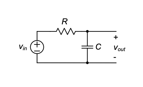
In this section, we will review important pre-requisite material using the RC circuit shown in Figure 3.1 as a driving example. Our objective is to gain insight into the circuit’s behavior when a sinusoidal signal of a given frequency is applied at its input. Since the circuit consists of linear elements, it follows that the output can only contain a sinusoid at the same frequency that is applied. Therefore, all we need to determine is the amplitude and phase of the output sinusoid. Note that even though we restrict ourselves to sine waves, the analysis results are generally useful since arbitrary periodic signals can be constructed from a sum of sinusoids
From first principles, we could approach this problem by applying \(KCL\) and \(KVL\), noting that the current flowing through a capacitor is given by \(C \cdot dv/dt\). The result of this analysis is a linear differential equation that links \(v_{in}(t)\) and \(v_{out}(t)\). This equation can be solved for a sinusoidal input, yielding in general two components that make up the output. The first is called the transient part; it decays to zero for \(t → ∞\) . The second is called the steady-state component, and it persists for all \(t\). This latter component is what we are interested in.
A convenient shortcut to obtain the steady-state response is to work with Laplace transform models for each circuit element and to determine the transfer functions in the \(s\)-domain. Once an \(s\)-transfer function is created, the circuit’s steady-state response to a sinusoidal input is found by letting \(s\) = \(j\omega\) and by computing the phase and the magnitude of the output as a function of frequency (\(\omega\)). The resulting characteristic is called the frequency response of the circuit and is usually plotted in the format of a Bode plot. The involved variables that capture how the magnitude and phase vary with frequency are called phase vectors or phasors. In this module, the notation for phasors uses an uppercase variable name and lowercase subscripts such as \(V_{in}\) and \(I_{out}\). We will now illustrate the flow of such an analysis using the \(RC\) circuit example
Example 3-1: Frequency Response of an RC Circuit
Find the magnitude and phase of the transfer function \(V_{out}\) /\(V_{in}\) in for the \(RC\) circuit in Figure 3.1.
SOLUTION
We begin by noting that in the \(s\)-domain, the reactance of a capacitor is given by \(1/sC\). By applying the voltage divider rule, we can therefore write a transfer function that links \(v_{out}\) and \(v_{in}\) in the \(s\)-domain as follows
\[ \frac{v_{out}}{v_{in}} = \frac{\frac{1}{sC}}{\frac{1}{sC} + R} = \frac{1}{1 + sRC} \]
In order to evaluate this transfer function for steady-state sinusoids, we let \(s\) = \(j\omega\) and obtain
\[ \frac{V_{out}}{V_{in}} = \left. \frac{v_{out}}{v_{in}}\right|_{s=j\omega} = \frac{1}{1+sRC} \]
Following the rules for determining the magnitude and phase of a complex number, we obtain
\[ \left| \frac{V_{out}}{V_{in}} \right| = \sqrt{\frac{1}{1 + (\omega RC)^2}} \]
and
\[ \angle \frac{V_{out}}{V_{in}} = \tan^{-1}(-\omega RC) \]
From this result, we see that for \(\omega RC \gg 1\) the sinusoid is attenuated and shifted by \(–90^\circ\), i.e.
\[ \left| \frac{V_{out}}{V_{in}} \right| = \frac{1}{\omega RC} \quad\quad\quad \angle \frac{V_{out}}{V_{in}} \simeq -90^\circ \]
For \(\omega RC \ll 1\), the sinusoid is passed unattenuated and with no phase shift, i.e.,
\[ \left| \frac{V_{out}}{V_{in}} \right| \simeq 1 \quad\quad\quad \angle \frac{V_{out}}{V_{in}} \simeq 0^\circ \]
This result makes intuitive sense, since the capacitor carries a larger current for high frequencies, increasingly “shorting” the output port and attenuating the signal. At high frequencies, the phase approaches \(–90^\circ\) due to the signal differentiation that takes place in the capacitor. Its current is given by \(C \cdot dv/dt\), and differentiation of a sine wave yields a cosine wave that is \(–90^\circ\) shifted in phase.
3.1.1 Bode Plots
In order to gain further insight from the magnitude and phase of a circuit, it is customary to plot the response in the form of a Bode plot, which shows the log of the magnitude versus the log of the frequency, and the phase angle versus the log of the frequency. In this representation, the magnitude and phase can be inspected over many orders of magnitude in frequency.
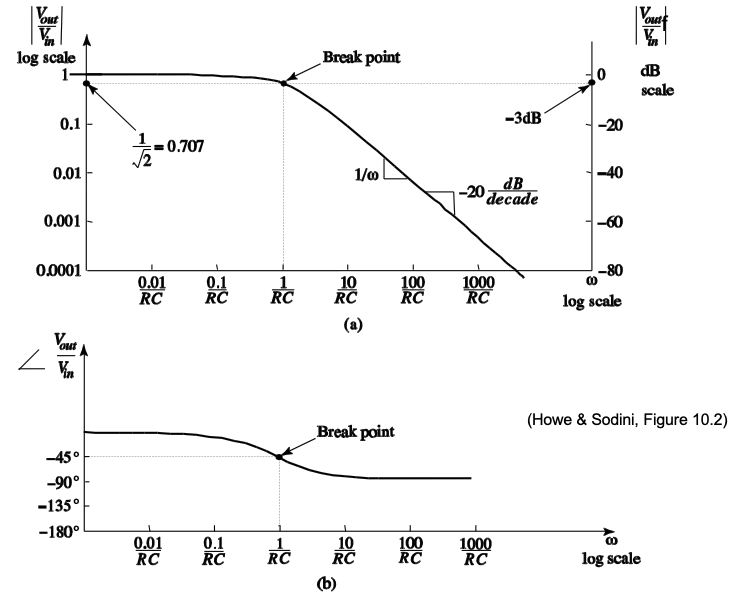
A Bode plot for the circuit of Figure 3.1 is shown in Figure 3.2. A few interesting features can be identified from this plot as follows. First, recall from the analysis of the circuit that for very high frequencies, where \(\omega \gg 1/RC\), the magnitude of the transfer function becomes inversely proportional to frequency. This is seen in the high-frequency region of the plot where the magnitude decreases by a factor of \(10\) for every factor of \(10\) increase in \(\omega\). Second, an interesting point in the Bode plot is where \(\omega= 1/RC\), also called the breakpoint frequency. At the breakpoint, the magnitude is given by
\[ \left| \frac{V_{out}}{V_{in}} \right| = \left| \frac{1}{1+j\omega RC} \right| = \left| \frac{1}{1+j} \right| = \frac{1}{\sqrt 2} = 0.707 \tag{3.1}\]
and the phase is
\[ \angle \frac{V_{out}}{V_{in}} = \tan^{-1}(-\omega RC) = \tan^{-1}(-1) = -45^\circ \tag{3.2}\]
It is customary to express the logarithmic magnitude scale on a Bode plot with a dimensionless unit called a decibel (dB). The magnitude of the ratio of voltages in units of dB is:
Ratio of voltages in decibels: \(20\ \log \left| \frac{V_{out}}{V_{in}} \right|\) dB
Therefore, in terms of decibels (indicated on the right-hand \(y\)-axis in Figure 3.2) the magnitude falls at –20 dB/decade at high frequencies. Expressed in decibels, the magnitude of the voltage at the breakpoint frequency \(\omega = 1/RC\) is \(20 \log (1/ \sqrt 2) \simeq -3\) dB.
The bandwidth of a circuit is a measure for the frequency range across which it exhibits only a small amount of attenuation. For a low-pass circuit (such as the RC circuit under investigation), the bandwidth is defined as the frequency for which the magnitude has dropped by a factor of \(1/\sqrt 2\) relative to its value at \(\omega = 0\) (DC gain). Since \(1/\sqrt 2\) corresponds to \(-3\) decibels, we refer to this quantity as the 3-dB bandwidth, or symbolically
\[ \omega_{3dB} = \frac{1}{RC} \tag{3.3}\]
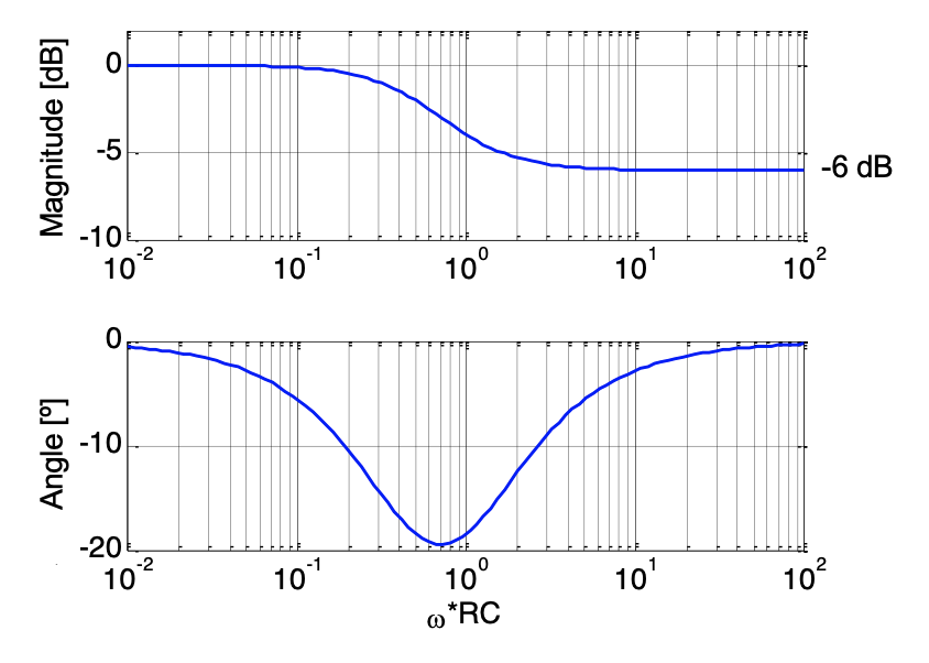
As an additional example, we will now look at the frequency response of the RC circuit with an additional resistor added in series with the capacitor \(C\), as shown in Figure 3.3.
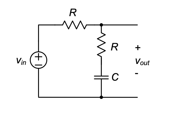
Example 3-2: RC Circuit with Additional Resistor
Find the magnitude and phase of the voltage transfer function for the circuit in Figure 3.3 and draw the corresponding Bode plot.
SOLUTION
By applying the voltage divider rule, we find
\[ \frac{v_{out}}{v_{in}} = \frac{\frac{1}{sC} + R }{\frac{1}{sC} + R + R} = \frac{1 + sRC}{1 + 2sRC} \]
Next, we let \(s = j\omega\) and obtain
\[ \frac{V_{out}}{V_{in}} = \left. \frac{v_{out}}{v_{in}}\right|_{s=j\omega} = \frac{1 + j\omega RC}{1 + 2 j\omega RC} \]
and finally
\[ \left| \frac{V_{out}}{V_{in}} \right| = \sqrt{ \frac{1 + (\omega RC)^2 }{1 + 2 (\omega RC)^2}} \]
and
\[ \angle \frac{V_{out}}{V_{in}} = \tan^{-1}(-\omega RC) + tan^{-1}(-2\omega RC) \]
The Bode plot for these expressions is found in Figure 3.4. As we can see, the plot is similar to the previous example in terms of the low-frequency behavior and first breakpoint. There is, however, a second breakpoint beyond which the magnitude approaches a constant value of \(–6\) dB (\(= 0.5\)), and the phase begins to return back to \(0^\circ\). This behavior is intuitively understood by inspection of the circuit. At high frequencies, the capacitor becomes a short, essentially leaving a resistive voltage divider. Since the resistors are of equal value, the voltage attenuation approaches \(0.5\) at high frequencies. Similarly, the phase returns to \(0^\circ\) because the resistive division at high frequencies has no impact on the signal’s phase.
3.1.2 Poles and Zeros
In linear system theory, poles and zeros are the \(s\)-values for which the value of the \(s\)-domain transfer function becomes infinity or zero, respectively. Since the behavior of a linear system is fully determined by the location of its poles and zeros, it is desirable to factor the transfer function in the following general format:
\[ H(s) = K \frac{\left( 1 - \frac{s}{z_1} \right) \left( 1 - \frac{s}{z_2} \right) \dots \left( 1 - \frac{s}{z_m} \right)}{\left( 1 - \frac{s}{p_1} \right) \left( 1 - \frac{s}{p_2} \right) \dots \left( 1 - \frac{s}{p_n} \right)} \tag{3.4}\]
where \(K\) is a constant DC gain term, \(p_1, p_2,... p_n\) are the poles and \(z_1, z_2,..., z_m\) are the zeros. For example, the \(s\)-domain transfer function of Example 3-2 is given by
\[ H(s) = \frac{v_{out}}{v_{in}} = \frac{\left( 1 - \frac{s}{z_1} \right)}{\left( 1 - \frac{s}{p_1} \right)} \tag{3.5}\]
where
\[ z_1 = -\frac{1}{RC} \quad and \quad p_1 = -\frac{1}{2RC} \tag{3.6}\]
The reason why \(p_1\) and \(z_1\) are called poles and zeros can be understood from the plot in Figure 3.5, which evaluates Equation 3.5 using the complex argument \(s = σ+ j\omega\). At \(s = p_1\), the magnitude of \(H(s)\) becomes infinite, resembling the pole of a tent holding up the 2-dimensional sheet in this representation. Likewise, at \(s = z_1\), the magnitude of \(H(s)\) becomes zero; this could be viewed as pegs pinning down the tent at this particular location.
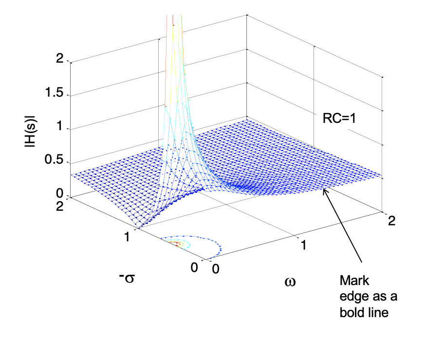
Since the steady-state magnitude response of the circuit is obtained by letting \(s = j\omega\), it simply corresponds to the bold line marked at the front edge of the plot. In other words, evaluating \(H(s)\) for the magnitude response corresponds to “walking” on the sheet of Figure 3.5 along the \(\omega\) axis.
As we can see from Equation 3.6, the poles and zeros of the example considered here are (negative) real numbers. For arbitrary ratios of polynomials in \(s\), the poles and zeros as expressed in Equation 3.4 can be complex numbers. For all circuits considered in this module, however, the poles and zeros will be real. Furthermore, all poles will be negative, as required for a stable system. The zeros encountered in this module can be either positive or negative as in 3.6. A negative zero is called a left half plane (LHP) zero, since it lies on the left side of the \(s\)-plane. A positive zero is called a right half plane (RHP) zero, since it lies on the right hand side of the \(s\)-plane.
When all the poles and zeros of a system are real, it is possible to create a set of rules that allow the construction of a bode plot by inspection. These rules are summarized in the next section.
3.1.3 Bode Plots of Arbitrary System Functions with Real Poles and Zeros
For the case of real negative poles and zeros, and letting \(s = j\omega\) , Equation 3.4 becomes
\[ H(j\omega) = K \frac{\left( 1 + j\frac{\omega}{\omega_{z1}} \right) \left( 1 + j\frac{\omega}{\omega_{z2}} \right) \dots \left( 1 + j\frac{\omega}{\omega_{zm}} \right)}{\left( 1 + j\frac{\omega}{\omega_{p1}} \right) \left( 1 + j\frac{\omega}{\omega_{p2}} \right) \dots \left( 1 + j\frac{\omega}{\omega_{pn}} \right)} \tag{3.7}\]
where \(\omega_{p1}, \omega_{p2},... \omega_{pn}\) are the pole frequencies and \(\omega_{z1}, \omega_{z2},..., \omega_{zm}\) are the zero frequencies. For instance, in Example 3-2, we have
\[ H(j\omega) = K \frac{\left( 1 + j\frac{\omega}{\omega_{z1}} \right) }{\left( 1 + j\frac{\omega}{\omega_{p1}} \right) } \tag{3.8}\]
where
\[ \omega_{z1} = \frac{1}{RC} \quad and \quad \omega_{p1} = \frac{1}{2RC} \tag{3.9}\]
To determine the Bode plot from Equation 3.7, we must assess the effect of each binomial term on the magnitude and phase of the system function. If the frequency is such that \(\omega \ll \omega_{zi}\) or \(\omega_{pi}\), then the respective binomial term will have little effect on the magnitude and phase of the system function, as it will simply multiply it by unity. On the other hand, if the frequency is such that \(\omega \ll \omega_{zi}\) or \(\omega_{pi}\), the system function, magnitude, and phase will be altered. To see this, we evaluate the magnitude and phase of a general binomial term for a left half plane pole or zero and \(\omega \gg \omega_i\)
\[ \left| 1 + j\frac{\omega}{\omega_i}\right| = \sqrt{1 + \left(\frac{\omega}{\omega_i}\right)^2} \simeq \frac{\omega}{\omega_i} \tag{3.10}\]
\[ \angle \left(1+ j \frac{\omega}{\omega_i}\right) = tan^{-1} \left(\frac{\omega}{\omega_i}\right) \simeq 90^\circ \tag{3.11}\]
Therefore, if the binomial term is in the numerator of the generalized system function (corresponding to a LHP zero), the magnitude will be multiplied by \({\omega}/{\omega_i}\), and a phase angle of \(90^\circ\) will be added to the total phase. If the binomial term is located in the denominator (LHP pole), the magnitude will be multiplied by \(1/({\omega}/{\omega_i})\) and a phase angle of \(90^\circ\) will be subtracted from the total phase. For a RHP zero, it follows that the magnitude will be multiplied by \({\omega}/{\omega_i}\), and a phase angle of \(90^\circ\) will be subtracted from the total phase.
When \(\omega = \omega_i\), the magnitude and phase are
\[ \left| 1 + j\frac{\omega}{\omega_i}\right| = |1+j| = \sqrt 2 \tag{3.12}\]
\[ \angle (1+j) = 45^\circ \tag{3.13}\]
Therefore, if these binomial terms for the breakpoints are located in the numerator, the magnitude of the system function in the numerator is multiplied by \(\sqrt 2\) and a phase of \(45^\circ\) is added to (for a LHP zero) or subtracted from (for a RHP zero) the overall phase. If it is located in the denominator, the magnitude is multiplied by \(1/\sqrt 2\) and a phase of \(45^\circ\) is subtracted from the overall phase of the system function.
Given these results, a Bode plot can be constructed by referring to the following step-by-step procedure.
- Identify all the breakpoint frequencies \(\omega_{pi}\) and \(\omega_{zi}\) and list them in increasing order. Apply the following rules, beginning with the lowest breakpoint frequency.
- If the corresponding binomial term appears in the numerator of the system function, the magnitude slope will be increased by \(20\) dB/decade, when the frequency is greater than the breakpoint frequency.
- If the corresponding binomial term appears in the denominator of the system function, the magnitude of the slope will be reduced by \(20\) dB/decade when the frequency is greater than the breakpoint frequency.
- To plot the phase, we know that the binomial term will contribute \(+45^\circ\) for a LHP zero, and \(-45^\circ\) for a RHP zero at \(\omega= \omega_i\). If it is in the denominator, it will contribute \(-45^\circ\). We assume that the \(\pm 90^\circ\) phase changes linearly over the interval \(0.1\omega i < \omega < 10\omega_i\).
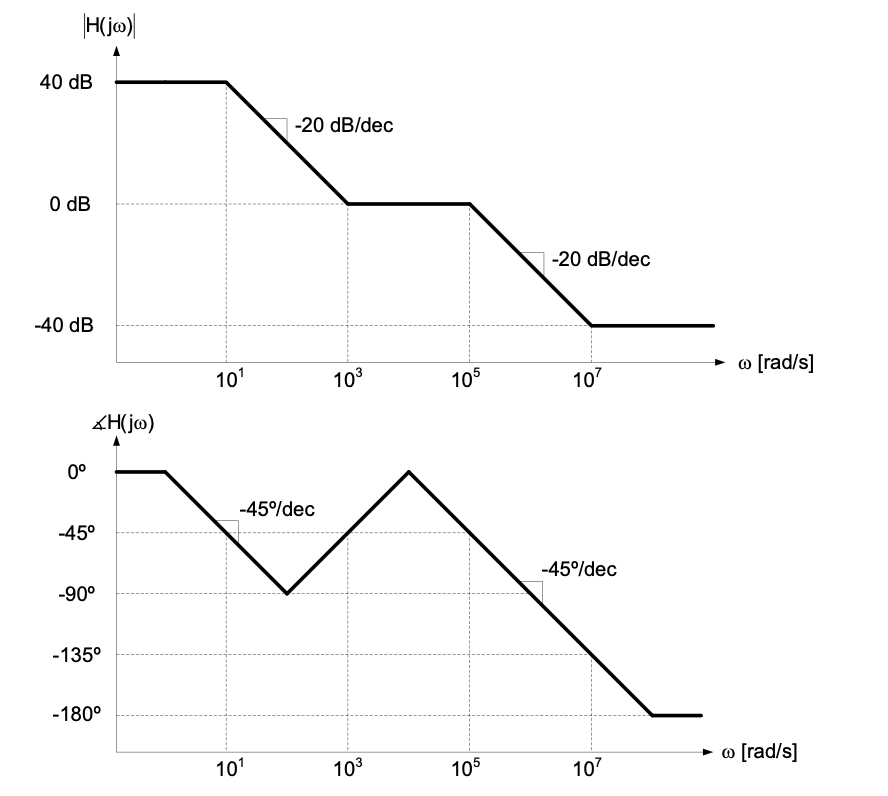
Example 3-3: Bode Plot Construction
Construct a Bode plot for a system with the following parameters: \(K = 100\), \(\omega_{p1} = 10\) \(rad/s\), \(\omega_{p2}\) = \(100\) \(krad/s\), left half plane zero: \(\omega_{z1}\) = \(1\) \(krad/s\), right half plane zero: \(\omega_{z2}\) = \(10\) \(Mrad/s\).
SOLUTION
First we note that the DC gain \(K = 100 = 40\) dB. Next we recognize that \(\omega_{p1}\) is the lowest frequency term, creating a change of slope in the magnitude plot toward \(–20\) dB/decade. The phase is \(0^\circ\) at the lowest frequency plotted, \(-45^\circ\) at \(\omega_{p1}\) and has reached \(-90^\circ\) at approximately \(10\) \(\omega_{p1}\). Applying the given rules in a similar fashion to the remaining poles and zeros yields the Bode plot shown in Figure 3.6.
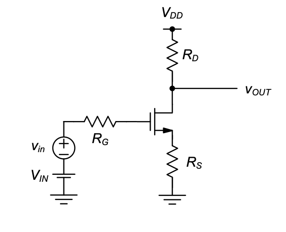
3.2 Frequency Response of the Common-Source Voltage Amplifier — First-Pass Analysis
We now wish to apply the analysis tools reviewed in the previous section to get a handle on the frequency response of the common-source voltage amplifier discussed in Chapter 2. Since the exact frequency behavior of this circuit is quite complex when taking all aspects into account, we partition this discussion into two steps. This section presents the first analysis step and uses the simplest possible model extension for the MOSFET that can be used to take capacitive effects, and thus frequency dependence, into account.
In the context of MOSFET capacitance modeling, it is useful to distinguish between intrinsic and extrinsic capacitances. Here, the term extrinsic refers to capacitances that are not needed to operate a MOSFET, but rather exist due to limitations or properties of a certain device structure or manufacturing process. As we shall see in Section 3-3, stray capacitances between the gate and source/drain terminals are examples of extrinsic capacitors. Intrinsic capacitance is unavoidable and required to operate the device. The oxide capacitance of a MOSFET falls into this category: without a capacitance between the gate and channel, no mobile charges can be induced (\(Q = CV\)), and the MOSFET would not function. In this section, we will look at frequency dependence effects due to the intrinsic capacitance only, beginning with a derivation of a circuit model that can be used to model this capacitance in the frequency response calculations.
3.2.1 Modeling Intrinsic MOSFET Capacitance
Just as in the derivation of device transconductance and output conductance, the operating point must be considered when calculating small-signal capacitances. We begin by analyzing the intrinsic capacitance of a MOSFET in the triode region, with its cross-section shown in Figure 3.7(a). To first-order, the gate and the conductive channel can be viewed as a parallel plate capacitor, resulting in a gate-to-channel capacitance of
\[ C_{gc} = WL \frac{\epsilon_{ox}}{t_{ox}} = WLC_{ox} \tag{3.14}\]
where \(WL\) is the capacitor plate area and \(C_{ox}\) is the oxide capacitance per unit area.
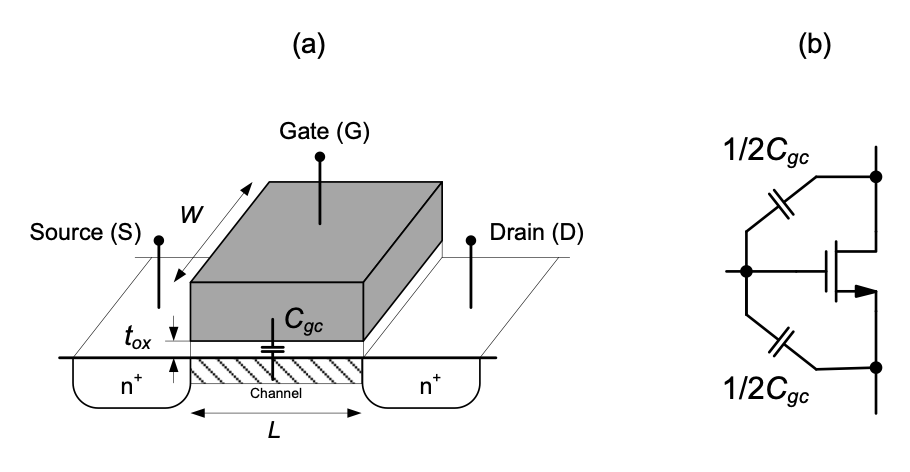
If the source and drain were connected together, the small signal capacitance from the gate to source/drain would be equal to \(C_{gc}\) as given in Equation 3.14. How can we model the capacitance when source and drain are not connected, i.e., how is the capacitance distributed between the two terminals?
A common first-order approximation is to assign half of \(C_{gc}\) to the capacitance between the gate and the source and the remaining half between the gate and the drain. This is schematically illustrated in Figure 3.7(b). A qualitative argument that supports this approximation is that small changes in either the drain or source voltage must induce the same change in charge at the gate; therefore, the capacitance must be split equally.
A case that is more relevant to the analysis of a common-source stage is the behavior in the saturation region. For this case, we know that the conductive channel does not extend all the way from the source to the drain, but is pinched off at some coordinate \(L – ΔL\). When the channel is pinched-off, the drain potential (to first-order) no longer influences the charge under the gate. Therefore, the intrinsic capacitance from the gate to the drain is approximately zero in this region of operation.
In saturation, the channel charge is therefore controlled primarily by the potential between the gate and the source, and a significant capacitance is present between these two terminals. At first glance, one might expect that \(C_{gs}\) is equal to \(C_{gc}\). However, this is not quite correct due to the pinch-off effect. Imagine applying a small voltage change to the source terminal. This will change the voltage across the oxide (and charge) near the source, but at the pinch-off point, the voltage across the oxide remains at \(V_{Tn}\). This means that the capacitance in the saturation egion must be less than \(C_{gc}\), because the charge does not see a uniform change as in the case of a simple parallel plate capacitor. Further analysis (see Reference 1) reveals that the capacitance between the gate and the source in the saturation region is given by
\[ C_{gs} = \frac{2}{3} C_{gc} = \frac{2}{3}WLC_{ox} \tag{3.15}\]
The resulting small-signal MOSFET model that includes this capacitance is shown in Figure 3.8.
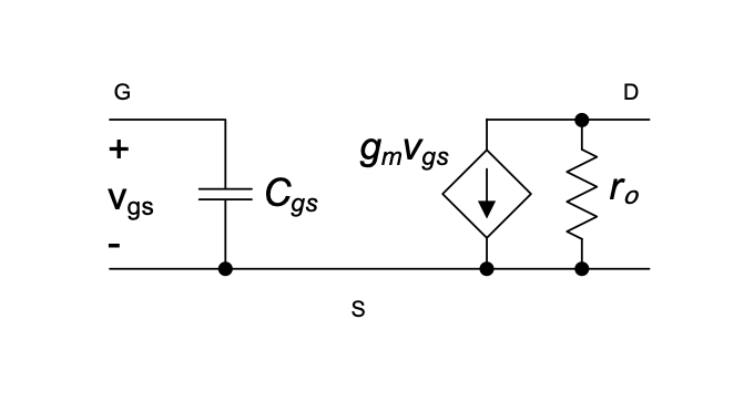
3.2.2 Frequency Response with Intrinsic Gate Capacitance
To analyze the frequency response of the common-source amplifier with the intrinsic gate capacitance, we insert the model of Figure 3.8 into the small-signal circuit model of the amplifier, as shown in Figure 3.9.
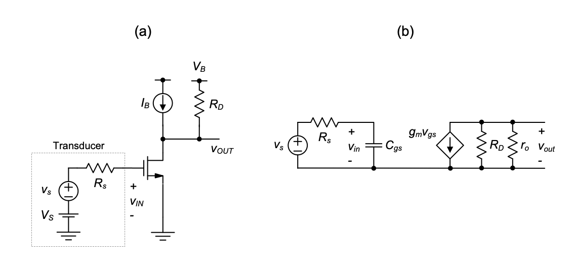
Note that if the circuit were driven by an ideal voltage source at its input port (\(v_{in}\)), the added capacitance would have no effect on the circuit’s operation. The ideal voltage source would provide any current that is needed to charge and discharge the gate capacitance without introducing any frequency dependence. The model in Figure 3.9 therefore considers a more realistic input source with finite resistance (\(R_s\)). At this point in the analysis, we purposely do not include any capacitive loading at the output of the amplifier, primarily to keep the first pass analysis simple and transparent.
In order to analyze the frequency response of the circuit in Figure 3.9, we first realize that the overall transfer function can be split into a product of two terms
\[ \frac{v_{out}}{v_s} = \frac{v_{out}}{v_{in}} \cdot \frac{v_{in}}{v_s} \tag{3.16}\]
In this expression, the first term on the right-hand side corresponds to the DC voltage gain given in Equation 2.51, and is equal to \(–g_mR_{out}\). The second term can be found by writing the voltage divider expression that relates node \(v_{in}\) to \(v_s\)
\[ \frac{v_{in}}{v_s} = \frac{\frac{1}{sC_{gs}}}{\frac{1}{sC_{gs}} + R_s} = \frac{1}{1+ sR_sC_{gs}} \tag{3.17}\]
With this result, the complete s-domain transfer function from the input source to the output becomes
\[ A_v(s) = \frac{v_{out}}{v_s} = \frac{-g_mR_{out}}{1 + sR_sC_{gs}} = \frac{A_{v0}}{1+ sR_sC_{gs}} \tag{3.18}\]
where \(A_{v0}\) = \(A_v(0)\) is a generalized placeholder for the DC gain of the circuit. From this result, we see that the transfer function has a DC gain corresponding to the result of Chapter 2, and a single pole that is set by the source resistance and the intrinsic gate capacitance. As explained in Section 3-1, we can now evaluate this transfer function for steady-state sinusoids by letting \(s = j\omega\) . This will allow us to draw a Bode plot and compute the bandwidth of the circuit.
Example 3-4: Common-Source Amplifier Bandwidth Calculation
Calculate the 3-dB bandwidth for the amplifier in Figure 3.9, assuming \(W\) = \(20 μm\), \(L\) = \(1 μm\), \(C_{ox}\) = \(2.3\) \(fF/μm^2\) and \(R_s = 50\) \(k\Omega\). Express the result in units of Hertz.
SOLUTION
For the given parameters, the gate-source capacitance is
\[ C_{gs} = \frac{2}{3} WLC_{ox} = 30.67 fF \]
The 3-dB bandwidth is
\[ \omega_{3dB} = \frac{1}{R_sC_{gs}} = 652.3 Mrad/s \]
and therefore
\[ f_{3dB} = \frac{\omega_{3dB}}{2\pi} = 103.8 MHz \]
An important question to ask at this point of the discussion is whether there is anything we can do to maximize the bandwidth of our amplifier. Assuming that we cannot change the source resistance \(R_s\), the only remaining option is to minimize \(C_{gs}\). This can be achieved by choosing a smaller transistor width or length [see Equation 3.15]. How will this affect the other performance metrics in the circuit? In the next subsection, we will show that there exists a direct tradeoff in the achievable bandwidth versus supply current for the circuit in consideration.
3.2.3 Tradeoff Between Bandwidth and Supply Current
Consider a design problem involving the circuit of Figure 3.9 and assume that the general objective is to maximize the circuit’s 3-dB bandwidth while minimizing the transistor’s drain current. For this analysis, we assume that \(R_s\), \(R_{out}\) and \(A_{v0}\) are given through specifications, and that these parameters cannot be varied. This assumption is not atypical in practical circuit design. \(R_s\) might be fixed by the physical properties of the input transducer. \(R_{out}\) could be set by an output resistance requirement that allows the circuit to interface with subsequent circuit stages, while the DC gain \(A_{v0}\) could be determined by application requirements. Furthermore, for simplicity, we neglect channel-length-modulation in this analysis.
In order to study the tradeoff between bandwidth and current consumption, we will now write expressions for these quantities that rely on common parameters. For the 3-dB bandwidth, we begin by inserting Equation 3.15 into Equation 3.15 and obtain
\[ \omega_{3dB} = \frac{3}{2} \cdot \frac{1}{R_sWLC_{ox}} \tag{3.19}\]
By using the following expression to eliminate \(C_{ox}\):
\[ g_m = \mu_n C_{ox} \frac{W}{L}(V_{GS}-V_{Tn}) = \mu_n C_{ox} \frac{W}{L}V_{OV} \tag{3.20}\]
and subsequently substituting \(g_m = |A_{v0}| / R_{out}\), Equation 3.19 becomes
\[ \omega_{3dB} = \frac{3}{2} \cdot \frac{\mu_n}{L^2}\cdot \frac{1}{|A_{v0}|} \cdot \frac{R_{out}}{R_s} \cdot V_{OV} \tag{3.21}\]
The above expression is now in a form that contains only technology parameters, design constraints (\(R_s, R_{out}\),and \(A_{v0}\)) and the gate overdrive voltage \(V_{OV}\) as a single design parameter. From this result, it is clear that in order to maximize bandwidth, we would like to use a technology that offers high mobility and short channels. The mobility is largely determined by material properties, while \(L\) is usually bounded by some \(L = L_{min}\) that is specific to a certain process technology, for example, \(1\) \(\mu m\) for the transistors used in this module.
From Equation 3.21, we also see that we should maximize \(V_{OV}\). However, a potential problem with this is due to the output signal range of the amplifier. As we know from Chapter 2, larger \(V_{OV}\) means that \(V_{DSsat}\) is also increased, and this means that the transistor enters the triode region at higher \(v_{OUT}\). This could lead to clipping, as discussed previously.
An additional, and more fundamental issue relates to the current consumption of the circuit. To see this, we rewrite Equation 2.31 as
\[ I_D = \frac{1}{2} \cdot g_m \cdot V_{OV} \tag{3.22}\]
and substitute \(g_m = |A_v| / R_{out}\) to find
\[ I_D = \frac{1}{2} \cdot \frac{|A_{v0}|}{R_{out}} \cdot V_{OV} \tag{3.23}\]
This result shows that a larger \(V_{OV}\) unfortunately requires a larger bias current for the transistor, and this is highly undesired in many applications, as for instance battery-powered devices.
While the above-observed tradeoff was discovered in the context of a particular circuit example, we will see throughout this module that the same tradeoff holds for all analog circuits. For a given technology and target specifications, current consumption directly scales with the circuit’s 3-dB bandwidth requirements. An alternative, and more general way to capture the fundamental connection between supply current and bandwidth is to inspect the tradeoffs that pertain to the MOSFET in isolation of a specific circuit example, as discussed next.
To begin, note that the model in Figure 3.8 comes with “desired” and “undesired” elements and properties. The only aspect of the transistor that we value is its transconductance. The associated intrinsic capacitance and the supply current needed to create the transconductance are undesired. Mathematically, we can identify the following figures of merit that capture the ratios between the desired and undesired quantities, in particular:
\[ \frac{g_m}{I_D}= \frac{2}{V_{OV}} \propto \frac{1}{\sqrt I_D} \tag{3.24}\]
and
\[ \frac{g_m}{C_{gs}} = \frac{3}{2} \cdot \frac{\mu_n}{L^2} \cdot V_{OV} \propto \sqrt I_D \tag{3.25}\]
The transconductance-to-current ratio, which is sometimes called the transconductance efficiency, deteriorates for larger \(V_{OV}\) (and larger \(I_D\)). On the other hand, the ratio of transconductance per intrinsic capacitance improves for larger \(V_{OV}\) (and larger \(I_D\)). This tradeoff is graphically illustrated in Figure 3.10. Note that as already pointed out in Section 2-2-7, the proportionality of \(g_m/I_D\) to \(1/V_{OV}\) extends only down to a certain minimum gate overdrive, defined as \(V_{OVmin}\) in this module [see Equation 2.35].
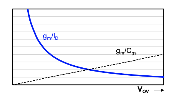
In essence, the gate overdrive voltage \(V_{OV}\) can be considered as a “knob” that lets us adjust the tradeoff between the two figures of merit. For a chosen \(V_{OV}\) and channel length, \(g_m / I_D\) and \(g_m / C_{gs}\) are fixed, and these parameters directly affect the speed and current consumption of the overall circuit. The gate overdrive \(V_{OV}\) has therefore been recognized by designers as an important parameter that affects most of the tradeoffs encountered in the optimization of a given circuit (see Reference 2). We will see examples of this throughout this module.
Interestingly, the product of the two figures of merit in Equation 3.24 and Equation 3.25 is given by
\[ \frac{g_m}{C_{gs}} \cdot \frac{g_m}{I_D} = 3 \cdot \frac{\mu_n}{L^2} \tag{3.26}\]
From this result, it is clear that for high speed and low current consumption, the best we can hope for is a technology that provides high mobility and short channels. In this context, it is interesting to note that improvements in device engineering and manufacturing processes have provided tremendous improvements in manufacturable channel lengths. Since the 1970s, \(L_{min}\) has been improved from \(10\) \(\mu m\) to approximately \(22\) \(nm\) today; a \(~400x\) reduction!
3.2.4 Transit Frequency
The figure of merit given in Equation 3.25 is also known as the transit frequency of the transistor and coincidentally quantifies the frequency for which the magnitude of the transistor’s current gain drops to unity. To determine the transit frequency, the transistor is operated in the common-source configuration and the input is driven by an ideal current source (see Figure 3.11). The output is short-circuited, and the current gain \(i_{out}/i_{in}\) is measured.
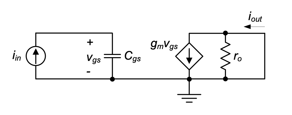
From the circuit, it follows that
\[ i_{out} = g_m \cdot v_{gs} = g_m \cdot \frac{i_{in}}{sC_{gs}} \tag{3.27}\]
Substituting \(s = j\omega\) and rearranging yields
\[ \frac{I_{out}}{I_{in}} = \frac{g_m}{j\omega C_{gs}} \tag{3.28}\]
The transit frequency then follows by setting
\[ \left| \frac{I_{out}}{I_{in}}\right| = 1 = \frac{g_m}{\omega_T C_{gs}} \tag{3.29}\]
and therefore
\[ \omega_T = \frac{g_m}{C_{gs}} \propto \sqrt{I_D} \tag{3.30}\]
The above quantity represents the transit frequency in rad/s. The symbol for the corresponding quantity in units of Hertz is \(f_T = \omega_T/2\pi\).
The transit frequency gives the designer a feel for the maximum frequency at which a circuit can operate. The bandwidth of most practical circuit configurations is limited to a fraction of \(\omega_T\), often about one order of magnitude below.
3.3 Frequency Response of the Common-Source Voltage Amplifier— Second-Pass Analysis
We will now extend the results from the previous section to obtain a more accurate understanding of the frequency response of a realistic common-source amplifier. To begin, we will extend the MOSFET model to include extrinsic capacitances.
3.3.1 Modeling Extrinsic MOSFET Capacitance
Figure 3.12 shows the cross section of a MOSFET device for further study of its associated capacitive elements. The first component of extrinsic capacitance that we will consider is called overlap capacitance; it is due to overlap of the source and drain diffusions and the gate and the contribution of the fringe electric fields from the gate. The overlap capacitance \(C_{ov}\) is quantified as a linear capacitance proportional to the gate width, with units of \(fF/\mu m\).
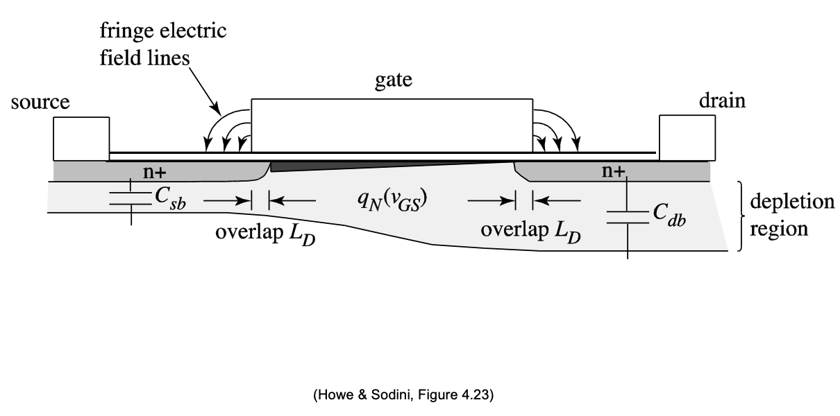
With overlap capacitance included, the total gate-source capacitance in saturation is the sum of Equation 3.15 and the overlap capacitance
\[ C_{gs} = \frac{2}{3} WLC_{ox} + WC_{OV} \tag{3.31}\]
Since the drain has no influence on the channel charge, the only contribution to the gate-drain capacitance is \(C_{OV}\)
\[ C_{gd} = WC_{OV} \tag{3.32}\]
In addition to the overlap capacitance, other extrinsic capacitance components are due to the reverse-biased junctions of the MOSFET. The drain-bulk and source-bulk capacitances \(C_{db}\) and \(C_{sb}\) indicated in Figure 3.12 originate from charge storage in the depletion regions between the drain and source n+ regions and the p-type bulk. The following expressions can be used to estimate these capacitances (see Reference 1 for a derivation):
\[ C_{db} = \frac{C_J \cdot AD}{(1+ V_{DB}/PB)^{MJ}} = \frac{C_{JSW} \cdot PD}{(1+ V_{DB}/PB)^{MJSW}} \tag{3.33}\]
\[ C_{sb} = \frac{C_J \cdot AS}{(1+ V_{SB}/PB)^{MJ}} = \frac{C_{JSW} \cdot PS}{(1+ V_{SB}/PB)^{MJSW}} \tag{3.34}\]
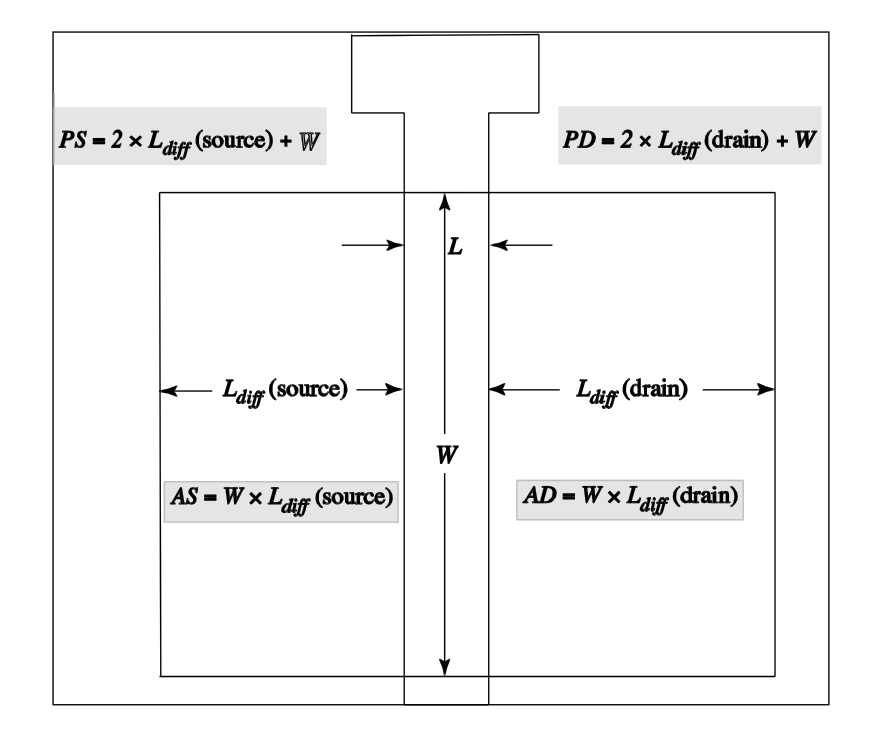
In these expressions, \(V_{DB}\) and \(V_{SB}\) are the reverse bias voltages of the junctions at the operating point. Note that with increasing reverse bias, the values of the junction capacitances decreases. The geometry parameters used in the expressions are related to the layout of the transistor as shown in Figure 3.13.
AD = Drain area
AS = Source area
PD = Perimeter of the drain diffusion (not including the edge under the gate)
PS = Perimeter of the source diffusion (not including the edge under the gate)
All other parameters are defined in Table 3-1 along with the technology parameters introduced thus far.
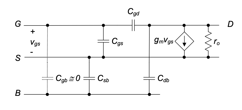
The extrinsic capacitances discussed above are added to the MOSFET small signal model as shown in Figure 3.14. For completeness, this model contains an additional capacitance \(C_{gb}\) between gate and bulk. This capacitance is due to the overlap of the polysilicon gate onto the field oxide region that isolates the MOSFET, as well as field lines from the gate terminating in the bulk of the transistor through the channel. This capacitance is usually small, and we will neglect it throughout this module.
Last, it is important to note that we have only modeled capacitances associated with the MOSFET, that is, the device without interconnections. The parasitic capacitances of the interconnections between MOSFETs can be a limiting factor and must be estimated from the layout and cross section for accurate analysis of a design. Off-chip wiring and package capacitances are also critical for evaluating the performance of any integrated circuit.
3.3.2 Transit Frequency with Extrinsic Capacitances
With extrinsic capacitances included in the model, the transit frequency expression of Equation 3.30 modifies to
\[ \omega_T = \frac{g_m}{C_{gs} + C_{gd}} \tag{3.35}\]
This can be seen by inserting the model of Figure 3.14 into the test setup of Figure 3.14. \(C_{sb}\) and \(C_{db}\) are shorted to ground (assuming the bulk terminal is also grounded), while \(C_{gd}\) appears in parallel with \(C{gs}\).
Example 3-5: Mosfet Capacitance Calculation
Consider an n-channel MOSFET biased in saturation with \(V_{DS}\) = \(2.5\) \(V\), \(I_D\) = \(500\) \(\mu A\), \(L\)= \(1\) \(\mu m\), and \(W\)= \(20\) \(\mu m\). Determine all the capacitances in the small-signal model of Figure 3.14, except the gate-bulk capacitance \(C_{gb}\) that we consider negligible. Also calculate the transistor’s transit frequency. Use the standard technology parameters defined in Table 3-1.
SOLUTION
Substituting \(C_{ox}\) and \(C_{ov}\) = \(0.5\) \(fF/\mu m\) into Equation 3.31, together with the MOSFET dimensions, we find
\[ C_{gs} = \frac{2}{3}(20 \cdot 1\mu m^2)\left(2.3\frac{fF}{\mu m^2}\right) + 20\mu m\left(0.5\frac{fF}{\mu m}\right) \]
\[ = 40.7fF \]
For the gate-drain capacitance, we obtain
\[ C_{gd} = 20 \mu m \left(0.5 \frac{fF}{\mu m}\right) = 10 fF \]
The remaining capacitances are the pn junction depletion capacitances \(C_{db}\) between the n+ drain and the substrate and \(C_{sb}\) between the n+ source and the substrate. Evaluating Equation 3.34, using the source junction bias voltage of \(V_{SB}\) = \(0\) \(V\) yields
\[ C_{sb} = 19fF \]
The drain junction has a bias voltage of \(V_{DB}\) = \(V_{OUT}\) = \(2.5\) \(V\). Evaluating Equation 3.33 with this value and the given parameters gives
\[ C_{db} = 11.6fF \]
Note that \(C_{db}\) is smaller than \(C_{sb}\) due to the larger reverse bias across the drain-bulk junction. To calculate the transit frequency, we first compute \(g_m\) using
\[ g_m = \sqrt {2\mu_n C_{ox}\frac{W}{L}I_D} \]
\[ = \sqrt {2\cdot 50\frac{\mu A}{V^2} \cdot \frac{20}{1} \cdot 500 \mu A } = 1 mS \]
Therefore
\[ f_T = \frac{1}{2\pi} \cdot \frac{g_m}{C_{gs} + C_{gd}} = \frac{1mS}{40.7fF + 10 fF} = 3.14GHz \]
| Parameter | n-channel MOSFET | p-channel MOSFET |
|---|---|---|
| Threshold voltage | \(V_{Tn}\) = 0.5V | \(V_{Tp}\) = -0.5V |
| Transconductance parameter | \(μ_nC_{ox}= 50μA/V^2\) | \(μ_pC_{ox}= 25μA/V^2\) |
| Chanel length modulation parameter | \(\lambda_n =0.1V^{-1}/L\) (\(L\) in \(\mu m\)) |
\(\lambda_p =0.1V^{-1}/L\) (\(L\) in \(\mu m\)) |
| Gate oxide capacitance per unit area | \(C_{ox} = 2.3fF/\mu m^2\) | |
| Overlap Capacitance | \(C_{ov} = 0.5fF/\mu m\) | |
| Zero-bias planar bulk depletion capacitance | \(C_{Jn} = 0.1fF/\mu m^2\) | \(C_{Jp} = 0.3fF/\mu m^2\) |
| Zero-bias sidewall bulk depletion capacitance | \(C_{JSWn}=0.5fF/\mu m\) | \(C_{JSWp}=0.35fF/\mu m\) |
| Bulk junction potential | \(PB = 0.95\) \(V\) | |
| Planar bulk junction grading coefficient | \(MJ = 0.5\) | |
| Sidewall bulk junction grading coefficient | \(MJSW = 0.33\) | |
| Length of source and drain diffusions | \(L_{diff} = 3\mu m\) | |
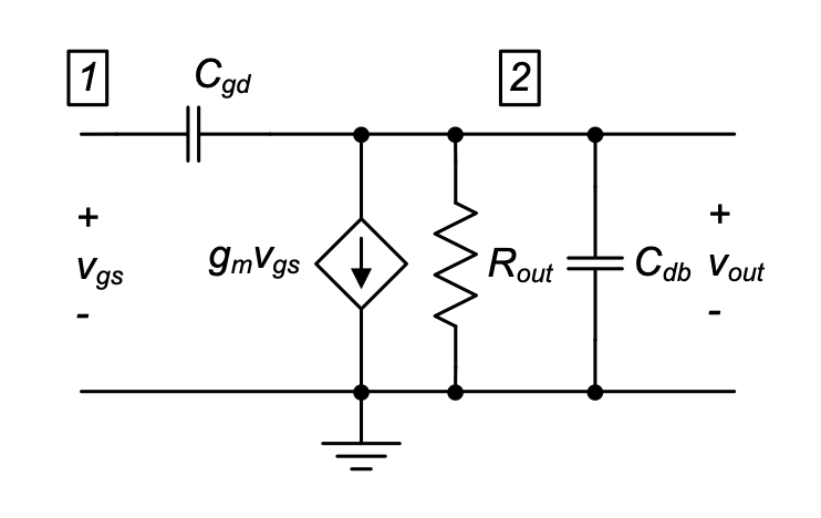
3.3.3 Frequency Response with Intrinsic and Extrinsic Gate Capacitances
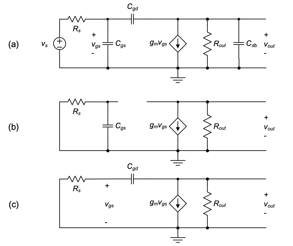
To analyze the frequency response of the common-source amplifier with intrinsic and extrinsic capacitances, we insert the model of Figure 3.14 into the small-signal circuit model of the amplifier, as shown in Figure 3.15(a). Note that we have neglected \(C_{gb}\) and also discarded \(C_{sb}\), since this capacitor has both terminals shorted to ground.
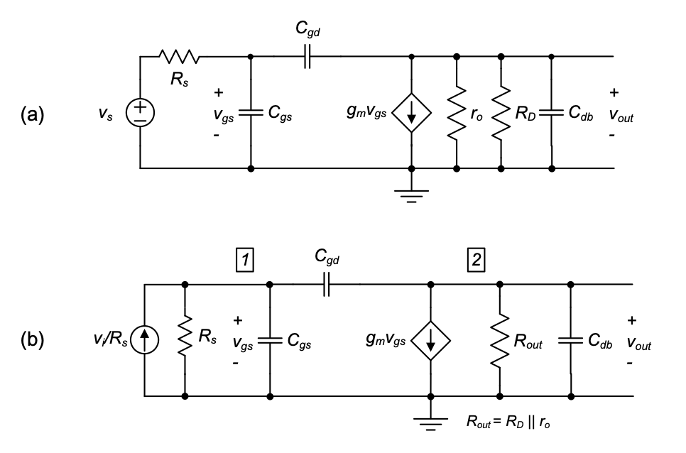
To simplify the full analysis of the amplifier, we redraw it as shown in Figure 3.15(b). We have taken the Norton equivalent at the input and combined the resistors at the input and output to reduce the number of terms carried in the algebra.
We begin the analysis by writing \(KCL\) at nodes 1 and 2
\[ 0 = -\frac{v_s}{R_s} + \frac{v_{gs}}{R_s} + v_{gs}sC_{gs} + (v_{gs} - v_{out})sC_{gd} \tag{3.36}\]
\[ 0 = g_m v_{gs} + sC_{gd}(v_{out} - v_{gs}) + \frac{v_{out}}{R_{out}} + sC_{db}v_{out} \tag{3.37}\]
Next, solving Equation 3.36 for \(v_{gs}\), substituting into Equation 3.37, and rearranging yields
\[ \frac{v_{out}}{v_s} = \frac{-g_m R_{out} \left( 1 - s\frac{C_{gd}}{g_m} \right)}{1 + b_1 s + b_2 s^2} \tag{3.38}\]
where
\[ b_1 = R_s \left( C_{gs} + C_{gd} \right) + R_{out} \left( C_{db} + C_{gd} \right) + g_m R_{out} R_s C_{gd} \tag{3.39}\]
and
\[ b_2 = R_s R_{out} \left( C_{gs}C_{gd} + C_{gs}C_{db} + C_{gd}C_{db} \right) \tag{3.40}\]
Although this result is algebraically complex, we can make a few preliminary observations about the terms in the numerator of Equation 3.38:
At DC (\(s = 0\), or all capacitors set to zero), the voltage gain of the circuit is \(–g_mR_{out}\), as we already concluded from the low-frequency analysis in Chapter 2.
The numerator contains a right half plane zero, \(z_1= g_m/C_{gd}\). Since obviously \(C_{gd} < C_{gs} + C_{gd}\), we conclude [via comparison with Equation 3.35] that this zero occurs at frequencies beyond \(\omega_T\), and is therefore irrelevant in many practical scenarios.
The denominator of the transfer function is a second-order polynomial in \(s\) with complicated dependencies on all component values. All we can say at first glance from inspecting the denominator is that we expect to see two poles in the frequency response of this circuit, because it can (in principle) be factored into two binomial terms. Note that this factorization would yield an even more complicated expression.
The main issue with a result of this complexity is that it cannot be understood intuitively. Consequently, it is difficult to recognize the main parameters that are limiting the performance, which in turn prevents the designer from identifying ways to optimize the circuit. Even though Equation 3.38 is mathematically exact, we would rather like to work with an expression that sacrifices some accuracy and/or detail in return for transparency and focus on the main effects that limit the performance. In order to take steps in this direction, we begin by evaluating Equation 3.38 numerically, primarily to get a feel for the pole locations in a typical circuit.
Example 3-6: Magnitude Response of the Common-Source Amplifier
Evaluate and plot the steady-state magnitude response of Equation 3.38 numerically using the following transistor parameters: \(g_m = 1\) \(mS\), \(C_{gs}\) = \(40.7\) \(fF\), \(C_{gd}\) = \(10\) \(fF\) and \(C_{db}\) = \(11.6\) \(fF\) (same as in Example 3-5). Assume \(R_{out}\) = \(5\) \(k\Omega\) and \(R_s\) = \(50\) \(k\Omega\). For comparison, also plot the magnitude response of Equation 3.18, i.e., considering only the intrinsic gate capacitance.
SOLUTION
The plots are generated by letting \(s = j\omega\) in Equation 3.38 and Equation 3.18, and subsequently plotting the magnitude of the expression as a function of frequency. The result is show in Figure 3.16. From the plots, we conclude the following:
In the response that uses intrinsic capacitance only, we see a pole at approximately \(100\) \(MHz\); this number corresponds to the value obtained in Example 3-4.
As expected, the response with both intrinsic and extrinsic capacitances exhibits two poles. More importantly, we see that one of the poles occurs at relatively low frequencies, while the other occurs at very high frequencies.
The low-frequency pole of the case with extrinsic capacitance included lies significantly lower than \(100\) \(MHz\). This tells us that extrinsic capacitance has a substantial impact on the bandwidth of this circuit.
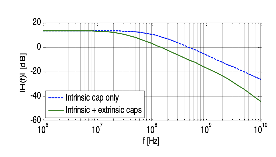
From the result of this particular example, we see that the bandwidth of the common-source amplifier is primarily set by a single pole that lies far from any other breakpoint in the response. In this case, we call the bandwidth limiting pole of the circuit the dominant pole. When a dominant pole condition exists, we would like to work with an expression of the form
\[ \frac{v_{out}}{v_s} = \frac{A_{v0}}{1-\frac{s}{p_1}} \tag{3.41}\]
instead of evaluating Equation 3.38. In some sense, Equation 3.38 contains too much information about irrelevant features of the response that have no impact on the 3-dB bandwidth. A commonly used technique that allows us to simplify expressions of the form of Equation 3.38 is therefore discussed in the next sub-section.
3.3.4 The Dominant Pole Approximation
In general, the denominator of the transfer function given in Equation 3.38 can be factored into two binomial terms
\[ \left(1-\frac{s}{p_1}\right)\left(1-\frac{s}{p_2}\right)= 1-s\left(\frac{1}{p_1}+ \frac{1}{p_2}\right) + \frac{s^2}{p_1p_2} \tag{3.42}\]
Furthermore, we know from our numerical evaluation of the previous subsection that the magnitude of one of the poles is much larger than the other, i.e
\[ |p_2| \gg |p_1| \tag{3.43}\]
and therefore
\[ |p_2| \ll |p_1| \tag{3.44}\]
Consequently, we can eliminate the second term in s on the right hand side of Equation 3.42 and approximate
\[ \left(1-\frac{s}{p_1}\right)\left(1-\frac{s}{p_2}\right)\simeq 1- \left(\frac{s}{p_1}\right) + \frac{s^2}{p_1p_2} \tag{3.45}\]
Now, comparing Equation 3.38 with Equation 3.45, we see that
\[ - \frac{1}{p_1} = b_1 \tag{3.46}\]
and thus
\[ p_1 = -\frac{1}{b_1} \]
\[ = - \frac{1}{R_s[C_{gs} + C_{gd}] + R_{out}[C_{db} + C_{gd}] + g_m R_{out} R_s C_{gd}} \]
\[ = - \frac{1}{R_s[C_{gs} + (1 + g_m R_{out})C_{gd}] + R_{out}[C_{db} + C_{gd}]} \tag{3.47}\]
This result gives us a relatively handy expression for the dominant pole in the common-source amplifier, and the bandwidth can be estimated using
\[ \omega_{3dB} = \frac{1}{R_s[C_{gs} + (1 + g_m R_{out})C_{gd}] + R_{out}[C_{db} + C_{gd}]} \tag{3.48}\]
As opposed to Equation 3.38, Equation 3.48 is much more useful for evaluating which particular component of the circuit may limit the bandwidth. Specifically, the term \((1 + g_mR_{out})C_{gd}\) looks like a potential problem. Whenever \(g_mR_{out}\) is large (high gain), this term may dominate the denominator of Equation 3.48, and therefore limit the bandwidth. This is a very important conclusion, but unfortunately took us many lines of algebra (including the derivation of Equation 3.38, which was not shown in detail) to develop. A more desirable approach would hint with very little algebra that the aforementioned term may limit the bandwidth. Such an approach is possible via the application of the Miller theorem and the Miller approximation, discussed in the next subsection.
3.3.5 The Miller Theorem and the Miller Approximation
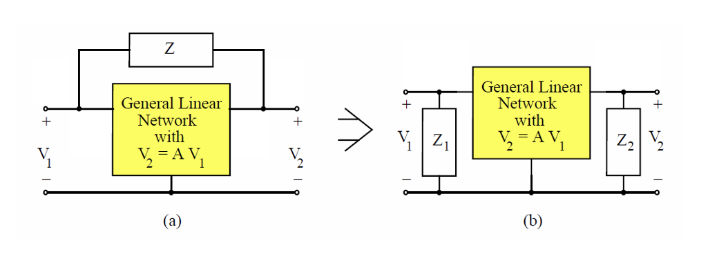
The Miller theorem is a general linear circuit theorem that can be used to replace an impedance connected between two circuit nodes by two impedances, connected from each terminal to ground. This is illustrated in Figure 3.17. The impedance \(Z\) in Figure 3.17(a) is replaced by the two impedances \(Z_1\) and \(Z_2\) in Figure 3.17(b). For the two circuits to be equivalent, it can be shown that
\[ Z_1 = \frac{Z}{1-A_{vM}} \quad and \quad Z_2 = \frac{A_{vM}Z}{A_{vM}-1} \tag{3.49}\]
where \(A_{vM} = V_2/V_1\) is the voltage gain across the impedance \(Z\), also called the Miller gain.
The Miller theorem is useful for the simplification of a variety of circuits. In the context of the common-source amplifier analysis in this chapter, we will use the theorem to eliminate the coupling of the output and input through \(C_{gd}\), and thereby arrive at a circuit that is easier to analyze and understand. Before applying the Miller Theorem to the full circuit model of Figure 3.15, we will first consider its application to an ideal voltage amplifier circuit with a coupling capacitance between the input and output, as drawn in Figure 3.18.
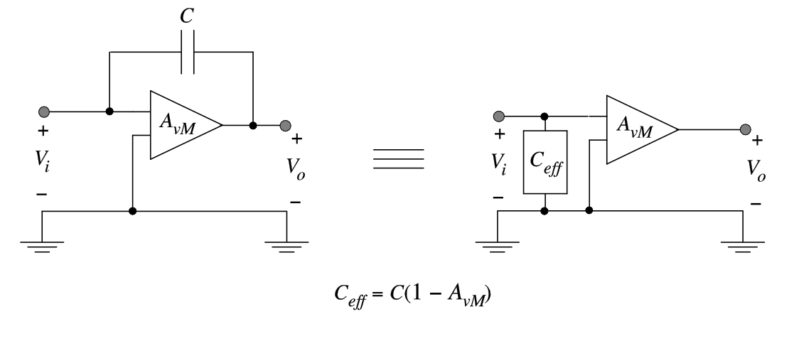
The goal of this example is to determine the effective shunt capacitance at the input port, when the signal is amplified by a gain of \(A_{vM}\) across the coupling capacitor \(C\). Using \(Z = 1/sC\), and \(Z_{eff} = 1/sC_{eff}\) we can apply Equation 3.49 to find
\[ \frac{1}{sC_{eff}} = \frac{\frac{1}{sC}}{1-A_{vM}} \tag{3.50}\]
and therefore
\[ C_{eff} = C(1- A_{vM}) \tag{3.51}\]
If the voltage gain \(A_{vM}\) is a negative number (as in the case of a common-source amplifier), the capacitance \(C\) is “amplified” by the factor \((1 + |A_{vM}|)\). Intuitively, without relying on a complete proof of the Miller Theorem, this result can be understood by examining the voltages and currents of the capacitor \(C\) in Figure 3.18. The voltage across \(C\) is
\[ v_C = v_{in} - v_{out} = v_in(1-A_{vM}) \tag{3.52}\]
and the current flowing into \(C\) from the input port is
\[ i_{in} = i_C = sCv_c = sC(1-A_{vM})v_in \]
\[ \frac{v_{in}}{v_{out}} = \frac{1}{sC(1-A_{vM})} = \frac{1}{sC_{eff}} \tag{3.53}\]
In essence, the capacitance is multiplied due to the large swing at the amplifier output; this increases the voltage across the capacitor and therefore forces a correspondingly multiplied current into the input port.
This result applies qualitatively also to the common-source amplifier studied in this chapter—i.e., the negative gain of the amplifier causes an amplification of \(C_{gd}\), which couples the input and output. However, a subtle difference is that the gain across the capacitor is not perfectly constant (as assumed above), but exhibits some frequency dependence.
To investigate, consider the circuit of Figure 3.19, which is the relevant section of the full common-source circuit needed to find the voltage gain across \(C_{gd}\). Applying KCL at node 2 and solving for \(A_{vM} = v_{out}/v_{gs}\) yields
\[ \frac{v_{out}}{v_{gs}} = -g_m R_{out} \left( \frac{1 - s \frac{C_{gd}}{g_m}}{1 + s R_{out}(C_{db} + C_{gd})} \right) \tag{3.54}\]
In this expression, the bracketed term contains a zero and a pole. The zero occurs beyond \(\omega_T\) and can be safely discarded. The situation is somewhat different for the pole. If \(R_{out}\) is very large, or if an additional load capacitance is added to the circuit output (in parallel with \(C_{db}\)), the pole can occur at relatively low frequencies, making the gain across \(C_{gd}\) non-constant in the frequency range of interest. Provided that the pole in the bracketed term occurs outside the frequency band of interest, we can assume
\[ \frac{v_{out}}{v_gs} \simeq -g_mR_{out} \tag{3.55}\]
This assumption is known as the Miller approximation, and it allows us to utilize the result from Equation 3.51, which assumed a constant gain across the capacitor in question.
To complete this discussion, we will now apply the Miller approximation to the model of the common-source amplifier in Figure 3.15. The result is shown in Figure 3.20. The capacitor \(C_{gd}\) is no longer connected between the input and output, but appears only across the input port, with its value multiplied by \((1+ g_mR_{out})\). From this model, the circuit bandwidth can be easily identified by inspection
\[ \omega_{3dB} = \frac{1}{R_s [C_{gs} + (1+g_mR_{out})C_{gd}]} \tag{3.56}\]

In comparison with Equation 3.48, this result is missing the term \(R_{out}(C_{gd} + C_{db})\) in the denominator. This is not surprising and also inconsequential when the Miller Approximation is applied properly. As we pointed out above, the Miller approximation is justified only when this time constant is small in the first place, ensuring a constant Miller gain in the band where the dominant pole is expected to lie. Whenever the Miller approximation is applied, it must be verified that the neglected pole in the Miller gain occurs far beyond the frequency estimated by Equation 3.56. This leads to the following procedure for the proper application of the Miller approximation in common-source amplifiers:
Calculate the low-frequency gain across \(C_{gd}\) and draw the simplified circuit model (as in Figure 3.20) with the Miller-amplified shunt capacitance at the input.
Estimate the bandwidth of the circuit using Equation 3.56.
Calculate the frequency of the pole in Equation 3.54. If and only if this pole frequency is far beyond the frequency calculated in step 2, the Miller approximation result is valid.
In a typical common-source circuit without a large load capacitance as drawn in Figure 3.20, the Miller approximation typically holds. When a very large capacitor is connected to the output, the approximation becomes invalid and the dominant pole is set by the \(RC\) time constant formed at the output.
Example 3-7 : Calculating the Common-Source Amplifier Bandwidth Using the Miller Approximation
Calculate the 3-dB bandwidth for the common-source voltage amplifier of Figure 3.15 using (a) the Miller approximation, and (b) the dominant pole approximation result of Equation 3.48. Parameters: \(g_m\) = \(1\) \(mS\), \(C_{gs}\) = \(40.7\) \(fF\), \(C_{gd}\) = \(10\) \(fF\), \(C_{db}\) = \(11.6\) \(fF\), \(R_{out}\) = \(5\) \(k\Omega\) and \(R_s\) = \(50\) \(k\Omega\) (same as in Example 3-6). Calculate the percent error in the result of part (a).
SOLUTION
- Using the Miller approximation [i.e., Equation 3.56], we obtain
\[ f_{3dB} = \frac{1}{2\pi} \cdot \frac{1}{R_s[C_{gs} + (1 + g_m R_{out})C_{gd}]} \] \[ = \frac{1}{2\pi} \cdot \frac{1}{50k\Omega[40.7{fF} + (1 + 1{mS} \cdot 5k\Omega)10{fF}]} \] \[ = 31.61{MHz} \]
- Using Equation 3.48 we find
\[ f_{3dB} = \frac{1}{2\pi} \cdot \frac{1}{R_s[C_{gs} + (1 + g_m R_{out})C_{gd}] + R_{out}[C_{db} + C_{gd}]} \] \[ = \frac{1}{2\pi} \cdot \frac{1}{50k\Omega[40.7{fF} + (1 + 1{mS} \cdot 5k\Omega)10{fF}] + 5k\Omega \cdot 21.6{fF}} \] \[ = 30.95{MHz} \]
The error in the result of part (a) is therefore
\[ \frac{31.61-30.95}{30.95} = 2.1\% \]
The error of \(2.1\%\) seen in this example is acceptable and will in practice be overshadowed by uncertainty in the transistor model parameters.
3.3.6 Calculating the Non-Dominant Pole*
The reader may wonder how the non-dominant pole frequency can be calculated within the above-discussed framework. A common misconception is to assume that after applying the Miller approximation, the non-dominant pole can be simply found from the time constant in the output network, i.e., \(R_{out}C_{db}\). This is incorrect, since the Miller approximation is not valid at the frequency where the non-dominant pole is located.
If a dominant pole condition exists, the proper way to estimate the non-dominant pole is by comparing the coefficients of Eqs. (3.45) and (3.38). Specifically, we utilize that
\[ \frac{1}{p_1p_2} = b_2 \tag{3.57}\]
and thus
\[ p_2 = \frac{1}{p_1 b_2} \] \[ = - \frac{R_s[C_{gs} + C_{gd}] + R_{out}[C_{db} + C_{gd}] + g_m R_{out} R_s C_{gd}}{R_s R_{out}(C_{gs} C_{gd} + C_{gs} C_{db} + C_{gd} C_{db})} \tag{3.58}\]
To simplify, let us assume that \(C_{gd}\) \(\ll\) \(C_{gs}\) and \(C_{gd} \ll C_{db}\). Note that the latter assumption is not strictly true based on typical values for the technology assumed in this module (see Example 3-5). However, if a load capacitance is added to the circuit, the approximation is more easily justified, with Cdb replaced by \(C_{db} + C_L\) (see Example 3-8), and we almost always have in practice \(C_{gd}\) \(\ll\) \(C_{db} +C_L\). Thus, under the stated conditions, we can write
\[ p_2 \simeq - \frac{R_sC_{gs}+R_{out}C_{db}+g_mR_{out}R_sC_{gd}}{R_sR_{out}C_{gs}C_{db}} \]
\[ = -\left ( \frac{1}{R_{out}C_{db}}+\frac{1}{R_sC_{gs}}+\frac{g_m}{C_{db}}\cdot \frac{C_{gd}}{C_{gs}}\right) \tag{3.59}\]
This approximate result indicates that the non-dominant pole lies at a frequency that is higher than \(1/R_{out}C_{db}\), especially when \(g_m\) is large. Note that Equation 3.59 essentially represents a “parallel combination” of time constants (analogous to parallel connections of resistors)—that is, the smallest time constant in the expression sets the pole frequency.
3.4 Open-Circuit Time Constant Analysis
3.4.1 General Framework
In Section 3-3-4, we derived an approximate expression for the 3-dB bandwidth of a common-source voltage amplifier, assuming that a dominant pole condition exists. In this analysis, we found that the bandwidth is fully determined by the coefficient \(b_1\) in the numerator of Equation 3.38.
The open-circuit time constant (OCT) analysis is a powerful and general technique that allows us to compute the term \(b_1\) for arbitrary circuits, without the need to derive the full circuit transfer function with all high-order artifacts included. More importantly, it breaks the analysis into small and computationally manageable steps that provide insight about which circuit elements present the main bandwidth bottleneck. The step-by-step procedure for applying the OCT analysis method can be summarized as follows (see Reference 3 for a derivation)
Remove all but one capacitor in the circuit that is to be analyzed. Let us call this capacitor \(C_j\).
Short all independent voltage sources and remove all independent current sources in the circuit.
Calculate the Thévenin resistance \(R_{Tj}\) seen by the capacitor \(C_j\) and compute the time constant \(\tau_{j0} = R_{Tj}C_j\). Here, the subscript “\(o\)” is used to emphasize the open-circuit condition.
Repeat the above steps 1-3 for all remaining capacitors in the circuit.
The sum of all time constants is exactly equal to \(b_1\). We can therefore estimate the circuit’s 3-dB bandwidth using
\[ \omega_{3dB} \simeq \frac{1}{b_1} \tag{3.60}\]
\[ b_1 = \sum_{{j=1}}^{{N}} \tau_{jo} \tag{3.61}\]
where \(N\) is the total number of capacitors in the circuit. The \(\tau_{jo}\) jo are called open-circuit time constants, because these were determined with all other capacitors open circuited.
Once a circuit is analyzed using the OCT method, we can see which of the individual open-circuit time constants is contributing most heavily to \(b_1\). To increase the bandwidth, we can try to redesign the circuit by lowering the Thévenin resistance or the capacitor value of that time constant.
3.4.2 OCT Analysis of a Common-Source Stage
Consider the common-source amplifier shown in Figure 3.21(a) as an example to further understand the method of open-circuit time constants. We begin by considering \(C_{gs}\) and therefore remove all other capacitors and short the input source as shown in Figure 3.21(b). As evident from this circuit, the Thévenin resistance seen by capacitor \(C_gs\) is \(R_S\) and the individual time constant contribution from \(C_{gs}\) is
\[ \tau_{gso} = R_SC_{gs} \tag{3.62}\]
Similarly, redrawing the circuit with only Cdb present will yield
\[ \tau_{dbo} = R_{out}C_{db} \tag{3.63}\]
Next, we determine the individual time constant contribution from capacitor \(C_{gd}\). To perform this calculation, we consider the circuit as redrawn in Figure 3.21(c). From this circuit, the Thévenin resistance seen across \(C_{gd}\) cannot be immediately determined by inspection. This is because of the \(g_m\) element, which couples the nodes to the left and right of the capacitance. We therefore resort to determining the Thévenin resistance from first principles, using a nodal analysis. As shown in Figure 3.22, we apply a test current source (\(i_t\)) and measure the resulting test voltage (\(v_t\)). Applying \(KVL\) and \(KCL\), we find that
\[ v_t = v_{gs} + R_{out}(g_mV_{gs} + i_t) \tag{3.64}\]
\[ v_{gs} = i_tR_S \tag{3.65}\]
After substituting Equation 3.65 into Equation 3.64, we obtain
\[ R_{Tgd} = \frac{v_t}{i_t} = R_S + R_{out}(g_mR_S+1) \]
\[ = R_S + R_{out} + g_mR_SR_{out} \tag{3.66}\]
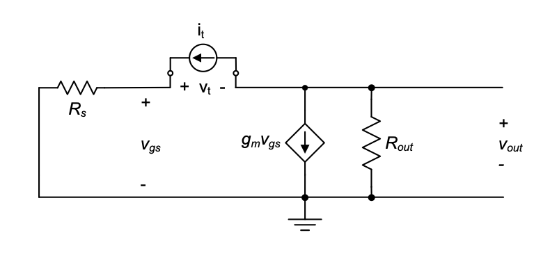
A common way to memorize this final result is “\(R_{left} + R_{right} + g_mR_{left} R_{right}\),” where \(R_{left}\) and \(R_{right}\) are the resistances seen to the left and right of the coupling capacitance \(C_{gd}\), respectively. Using this result, the individual time constant resulting from \(C_{gd}\) is given by
\[ \tau_{gdo} = R_{Tgd}C_{gd} = [R_S+R_{out}+g_mR_SR_{out}]C_{gd} \tag{3.67}\]
Next, we add the individual time constants from Equation 3.62, Equation 3.63, and Equation 3.67, which results in
\[ b_1 = R_S[C_{gs} + C_{gd}] + R_{out}[C_{db}+C_{gd}] + g_mR_{out}R_SC_gd \] \[ = R_S[C_{gs}+(1+g_mR_{out})C_{gd}] + R_{out} [ C_{db}+ C_{gd}] \tag{3.68}\]
Note that this result is identical to Equation 3.39, which was obtained from an exact nodal analysis of the complete circuit. This verifies that the method of open-circuit time constants is an exact analysis to determine the factor \(b_1\), which multiplies the first-order term in \(s\) in the denominator of the generalized system function. As before, the resulting estimate of the 3-dB breakpoint frequency is therefore given by
\[ \omega_{3dB} = \frac{1}{b_1} \] \[ = \frac{1}{R_S[C_{gs}+(1+g_mR_{out})C_{gd}] + R_{out} [ C_{db}+ C_{gd}]} \tag{3.69}\]
It is important to remember that this result maintains good accuracy only if a dominant pole condition exists. As we showed in Section 3-3-4, this condition is required so that we can approximate \(\omega_{3dB} \simeq 1/b_1\). Finally it is worth noting that Equation 3.69 shows that \(C_{gd}\) is effectively multiplied by the circuit’s voltage gain; this corresponds to the Miller amplification effect discussed in the previous section.
A simple example where the dominant pole condition is not met is shown in Figure 3.23. The reader may prove that the exact transfer function of this circuit is
\[ \frac{v_{out}}{v_s} = \frac{-g_mR}{(1+sRC)(1+sRC)} \tag{3.70}\]
and thus
\[ |p_2| = |p_1| = \frac{1}{RC} \tag{3.71}\]
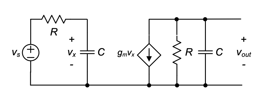
Therefore, we expect that the approximation of Equation 3.45 cannot be applied and \(1/b_1\) will not be a good estimate for the circuit’s bandwidth. It is now interesting to calculate the error that will result if the OCT method is nonetheless “blindly” applied.
In performing the OCT analysis, we see that the circuit in question has two open-circuit time constants equal to \(RC\). The bandwidth estimate using OCT analysis is therefore
\[ \omega_{3dB,OCT} \simeq \frac{1}{b_1} = \frac{1}{2RC} \tag{3.72}\]
On the other hand, we can find the exact 3-dB frequency of the circuit using
\[ \frac{1}{\sqrt 2} = \left| \frac{1}{(1+j\omega_{3dB}RC)(1+j\omega_{3dB}RC)}\right | \tag{3.73}\]
Solving for \(\omega_{3dB}\) gives
\[ \omega_{3dB} = \frac{1}{RC} \sqrt{\sqrt{2} -1} \simeq \frac{0.64}{RC} \tag{3.74}\]
The error in the OCT estimate is thus
\[ \frac{0.5 - 0.64}{0.64} = -22\% \tag{3.75}\]
From this result, we can draw a few interesting conclusions. First, even though the dominant pole condition is grossly violated in the above example, the OCT analysis is not extremely far off from the exact result. Second, the OCT result is conservative in the sense that it tends to underestimate the circuit’s bandwidth. This is desirable since the designer can rest assured that the bandwidth is at least as large as predicted by the OCT analysis. It can be shown that this latter property holds for arbitrary circuits whose poles lie on (or near) the real axis, and whose zeros occur beyond the estimated \(\omega_{3dB}\). This is the case for most circuits considered in this module. We will highlight exceptions where appropriate.
In summary, the reader should remember the following key points when applying the OCT analysis:
In any circuit, the sum of the open-circuit time constants corresponds (exactly) to the term \(b_1\), which multiplies the first-order term in the denominator of the circuit’s \(s\)-domain transfer function.
Under the following conditions, the bandwidth of the circuit can be approximated with good accuracy by \(1/b_1\): (1) a dominant pole condition exists, (2) the transfer function contains only poles that lie on (or near) the real axis, and (3) the zeros in the transfer function occur beyond the bandwidth estimate in question.
Even if no clear dominant pole condition exists, OCTs can be used to get a first-order feel for the bandwidth of a circuit. For instance, in a circuit with two identical real poles, the OCT bandwidth estimate is in error by \(–22\%\). As long as condition (2) above is met, the percent error will be negative and thus the estimated bandwidth is at least as large as the actual bandwidth (measured, e.g., using a circuit simulation).
Open-circuit time constants, in general, do not necessarily correspond to the poles of a circuit. The OCT correspond to poles only in circuits that can be broken into decoupled \(RC\) sections, as is the case in the circuit of Figure 3.23.
Example 3-8 Common-Source Amplifier Bandwidth Estimate Using an OCT Analysis
Consider the circuit shown in Figure 3.24 and assume the following parameters: \(W = 20 \, \mu{m}\), \(L = 1 \, \mu{m}\), \(I_B = 500 \, \mu{A}\), \(g_m = 1 \, {mS}\), \(C_{gs} = 40.7 \,{fF}\), \(C_{gd} = 10 \, {fF}\), \(C_{db} = 11.6 \, {fF}\), \(R_{out} = R_D \parallel r_o = 5 \, {k}\Omega\) and \(R_s = 50 \, {k}\Omega\) (same as in Example 3-7). The value of the load capacitance is \(C_L = 10 \, {pF}\). Estimate the \(3\)-dB bandwidth using an OCT analysis and propose a design modification that will increase the bandwidth by \(20\%\). For this modification, you may not alter the circuit’s DC gain, and \(R_S\) and \(C_L\) must be kept constant.
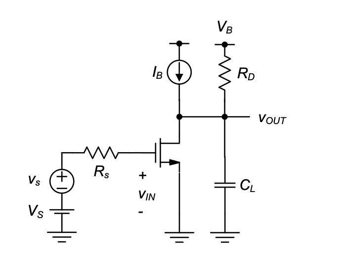
SOLUTION
The circuit has three open-circuit time constants as expressed in Equation 3.62, Equation 3.63, and Equation 3.67, with the difference that \(C_L\) appears in parallel to \(C_{db}\). The three OCT expressions are therefore
\[ \tau_{gso} = R_SC_{gs} \] \[ \tau_{dbo}^{\prime} = R_{out}(C_{db} + C_L) \]
\[ \tau_{gdo} = R_{Tgd}C_{gd} = [R_S+R_{out}+g_mR_SR_{out}]C_{gd} \]
Evaluating these expression with the given numbers yields
\[ \tau_{gso} = 50k\Omega \cdot 40.7fF= 2.035ns \]
\[ \tau_{dbo}^{\prime} = 5k\Omega (11.6pF + 10pF) = 50.01ns \]
\[ \tau_{gdo} = [50k\Omega +5k\Omega + 1mS \cdot 5k\Omega \cdot 50k\Omega]10fF \]
\[ = 3.05 ns \]
The bandwidth estimate is
\[ f_{3dB} = \frac{1}{2\pi} \cdot \frac{1}{2.035ns + 50.01ns + 3.05ns} = 2.89MHz \]
In order to improve the bandwidth by \(20\%\), it is clear that we must reduce the dominant open-circuit time constant \(\tau_{dbo}^{\prime}\). Since \(C_L\) must remain unchanged, the only option is to reduce Rout. To first-order, reducing Rout to approximately \(4\) \(k\Omega\) (a \(20\%\) reduction from the original value of \(5\) \(k\Omega\)) should get us close to the desired improvement. In order to keep the DC gain of the circuit constant, we now require a larger transconductance
\[ g_m = \frac{A_{v0}}{R_{out}} = \frac{5}{4k\Omega} = 1.2mS \]
There are several ways to increase the transconductance of the MOSFET. (i) Keep the device width constant and increase the bias current \(I_D\). An advantage of this option is that none of the device capacitances will change, thereby avoiding any counterproductive increase in the total time constant.(ii) Keep \(I_D\) constant and increase the device width \(W\). This option has the advantage that the current consumption of the circuit will not increase. Finally, option (iii) is to increase both \(W\) and \(I_D\) by the same factor. This option has the advantage that the gate overdrive voltage \(V_{OV}\) remains unchanged, and hence the input bias voltage and output voltage swing are unaffected. Since our primary focus in this example is to improve bandwidth, and current consumption and biasing considerations are secondary, we will apply option (i).
Using Equation 2.30, the new value of the required \(I_B\) is
\[ I_B = I_D = \frac{g_m^2}{2\mu_n C_{ox} \frac{W}{L}} = \frac{(1.2mS)^2}{2 \cdot 50\frac{\mu A}{V^2} \cdot \frac{20}{1}} = 720\mu A \]
Note that this value is approximately \(44\%\) larger than the original bias current of \(500\) \(\mu\)\(A\).
As a final verification step, we recompute the bandwidth estimate using the new value of Rout. The time constant \(\tau_{gso}\) remains the same, while the change in \(\tau_{gdo}\) is negligible. The dominant OCT modifies as follows
\[ \tau_{dbo}^{\prime} = 4k\Omega (11.6fF + 10pF) = 40.05ns \]
The modified bandwidth estimate is therefore
\[ f_{3dB} = \frac{1}{2\pi} \cdot \frac{1}{2.035ns + 40.05ns + 3.05ns} = 3.53MHz \]
which is about \(22\%\) larger than the original bandwidth, satisfying our design intent.
3.4.3 OCT Extensions
The OCT analysis covered in this section is tailored toward finding the upper corner frequency in circuits that are limited by capacitive elements; this is the most common situation encountered in integrated circuit design. For completeness, it is worth mentioning that there exists a method of short-circuit time constants (see Reference 3), which aims at estimating the lower corner frequency of a circuit with a high-pass characteristic. This is useful for circuits that employ AC coupling of various forms.
In circuits that contain inductors, the additional time constants can be included by shorting all but one inductor at a time. The generalized framework that includes the consideration of both inductors and capacitors to estimate the upper corner frequency of a circuit is called zero-value time constant analysis. Finally, it is interesting to note that higher-order terms [such as \(b_2\) in Equation 3.40] can be found using an OCT-like analysis. The interested reader is referred to Reference 4 for a comprehensive discussion of such methods.
3.4.4 Time Constants versus Poles
The distinction between open-circuit time constants and poles tends to be a source of confusion among circuit design students. We will therefore review the differences in this section using two examples.
Consider first the circuit of Figure 3.23. As we have shown above, this circuit has two open-circuit time constants, equal to \(RC\). Also we found that this circuit has two poles, located at \(–1/RC\). Thus, in this particular circuit, the poles coincide with the (reciprocals of the) time constants. The reason for this coincidence is that the two networks at the input and output are fully decoupled and represent simple first order \(RC\) sections. For such a topology, the circuit designer sometimes loosely speaks of a “pole at the input” and “pole at the output,” which are directly set by the time constants of each network.
Consider now the circuit of Figure 3.25, which is the same as Figure 3.23, except that we have added an additional capacitor \(C\) between the input and output terminal. This circuit retains the two open-circuit time constants of the original circuit (equal to \(RC\)), but has an additional one due to the added capacitor, equal to \(RC(2 + g_mR)\). On the other hand, the poles of this circuit can no longer be found by inspection. The transfer function has the form of Equation 3.38, with \(b_1 = RC(4 + g_mR)\) and \(b_2 = 3(RC)^2\). The two poles of the circuit are the roots of the denominator polynomial \(1 + b_1s + b_2s^2 = 0\) and their value depends on the value of \(g_mR\). Assuming \(g_mR = 2\) as a numerical example, the roots, and therefore the poles become
\[ p_{1,2} = - \frac{1}{RC}\left(1\pm \sqrt{\frac{2}{3}}\right) \tag{3.76}\]
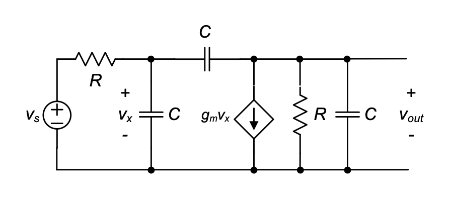
As we can see from this result, the poles do not coincide with any of the open-circuit time constants. More significantly, the number of poles (two) is not even equal to the number of open-circuit time constants (three).
As we can see from this result, the poles do not coincide with any of the open-circuit time constants. More significantly, the number of poles (two) is not even equal to the number of open-circuit time constants (three).
Finally, to fully close the loop between the two analysis techniques, note that the magnitude of the low-frequency pole in Equation 3.76 is approximately equal to \(0.18/RC\). This is close to the 3-dB bandwidth predicted by the sum of the open-circuit time constants (for \(g_mR = 2\)): \(1/(4RC + RC + RC) = 0.167/RC\), which, as expected, is slightly conservative.
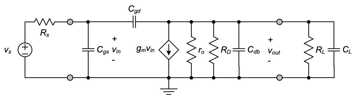
3.5 High-Frequency Two-Port Model for the Common-Source Voltage Amplifier
To summarize, Figure 3.26 shows the most general two-port model for the common-source voltage amplifier [similar to Figure 3.15] with source and load networks included. The advantage of this model representation is that it is valid for arbitrary component values. The disadvantage is that analyzing a circuit based on this model leads to complex equations. Generally, one should use this model as the starting point for the analysis of more complex circuits that contain a CS amplifier (see Chapter 6). Then, whenever suitable, we can invoke simplifications such as the Miller approximation or open-circuit time constants to simplify the analysis.
Finally, note that the model of Figure 3.26 is not well suited for a translation into a native voltage amplifier model (using a voltage controlled voltage source) as done for the low-frequency circuit in Section 2-4. The capacitors connected to the output port would lead to a frequency-dependent open-circuit gain and output impedance (\(Z_{out}\) rather than \(R_{out}\)) that give a non-intuitive representation of the circuit. It is therefore preferred to describe this voltage amplifier using the transconductance model as shown.
3.6 Summary
In this chapter we have reviewed the basic concepts of frequency domain analysis and introduced the intrinsic and extrinsic device capacitances of a MOSFET. Using the obtained small-signal model, the frequency response of any circuit can be obtained from first principles using the following steps:
Derive the transfer function using a nodal analysis.
Let and solve for the magnitude of the \(s=j\omega\) resulting expression.
Set the magnitude equal to \(1/\sqrt 2\) times the DC gain value, and solve for \(\omega\).
Unfortunately, this method is algebraically too complex for all but the most basic circuits. Consequently, we introduced several approximate methods and tools that are frequently used by analog circuit designers. These methods were developed using our driving example of a common-source voltage amplifier, but are widely used in other situations as well
Provided that an exact (and potentially complicated) transfer function expression is available, the dominant pole approximation can be applied to arrive at a simplified bandwidth expression. In this approximation, it is assumed that a single pole dominates the response and sets the circuit’s 3-dB bandwidth.
The Miller approximation was used to obtain a quick estimate of the 3 -dB bandwidth specifically for the common-source voltage amplifier. Although it is not an exact calculation, it is very useful for determining an estimate of the bandwidth of the amplifier analytically. Furthermore, this analysis gave insight into the effect of “Miller-multiplication” of a capacitor that appears across a voltage gain path. This effect is found in a multitude of circuits, and understanding this mechanism is insightful for design.
The method of open-circuit time constants is the most powerful and most broadly applicable technique discussed in this chapter. It provides an accurate answer for the circuit’s bandwidth if a dominant pole condition exists. Even if the dominant pole condition is not strictly met, the method yields acceptable errors (on the conservative side) on the order of a few tens of percent, which is often acceptable in a first-order hand analysis. Finally, the method of open-circuit time constants is an excellent design tool since it assists in finding which capacitors and Thévenin resistances are dominating the dynamic performance.
3.7 References
R. F. Pierret, Semiconductor Device Fundamentals, Prentice Hall, 1995.
D. K. Shaeffer and T. H. Lee, “A 1.5 V, 1.5 GHz CMOS low noise amplifier,” IEEE J. Solid-State Circuits, pp. 745–759, May 1997.
P. E. Gray and C. L. Searle, Electronic Principles Physics, Models, and Circuits, Wiley, 1969.
A. Hajimiri, “Generalized Time- and Transfer-Constant Circuit Analysis,” IEEE Trans. Circuits and Systems I, Vol. 27, No. 6, pp. 1105–1121, June 2010.
3.8 Problems
Unless otherwise stated, use the standard model parameters specified in Table 3-1 for the problems given below. Consider only first-order MOSFET behavior and include channel-length modulation (as well as any other second-order effects) only where explicitly stated.
P3.1 Sketch the Bode plots (magnitude and phase) for the following transfer functions. Assume \(R_iC_i \gg R_kC_k\) if \(i > k\).
\([1 / (1 + j\omega R_1 C_1)] [(1 / (1 + j\omega R_2 C_2))]\)
\((j\omega R_3 C_3) [(1 + j\omega R_4 C_4) / (1 + j\omega R_5 C_5)]\)
\([(1 + j\omega R_6 C_6) / (1 + j\omega R_8 C_8)] [(1 + j\omega R_7 C_7) / (1 + j\omega R_9 C_9)]\)
P3.2 A system has a DC gain of 500, LHP zeros at \(10\) \(kHz\) and \(1\) \(MHz\) and LHP poles at \(100\) \(kHz\), \(10\) \(MHz\), and \(100\) \(MHz\).
Write the \(s\)-domain transfer function that describes this system.
Draw a Bode plot for both the magnitude and phase of this system.
Switch the poles and zeros and repeat parts (a) and (b).
P3.3 Sketch the Bode plot for the magnitude, \(|I_o /I_s|_{dB}\) and phase \(\angle I_o/I_s\) of the circuit shown in Figure 3.27, given
\(R_1\) = \(10\) \(k\Omega\), \(R_2\) = \(100\) \(k\Omega\), \(C = 1\) \(pF\)
\(R_1\) = \(0.1\) \(k\Omega\), \(R_2\) = \(100\) \(k\Omega\), \(C = 1\) \(pF\)
\(R_1\) = \(10\) \(k\Omega\), \(R_2\) = \(100\) \(k\Omega\), \(C = 10\) \(pF\)
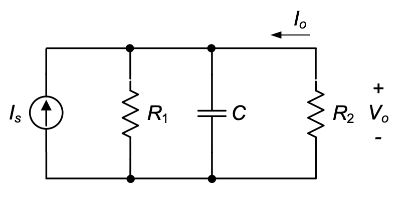
P3.4 Repeat Example 3-5 for the following parameters (assuming \(V_{DS}\) = \(2.5\) \(V\)). For each case, compute by which factor the transistor’s transit frequency has changed relative to the value seen in Example 3-5.
- \(I_D = 500\) \(\mu A\), \(L= 2\) \(\mu m\), and \(W= 20\) \(\mu m\).
- \(I_D = 500\) \(\mu A\), \(L= 1\) \(\mu m\), and \(W= 40\) \(\mu m\).
- \(I_D = 1000\) \(\mu A\), \(L= 1\) \(\mu m\), and \(W= 40\) \(\mu m\).
P3.5 Repeat Example 3-5 for a p-channel MOSFET operating in saturation. Parameters: \(V_{SD} = 2.5\) \(V\), \(–I_D = 500\) \(\mu A\), \(L= 1\) \(\mu m\), and \(W= 20\) \(\mu m\). Compute the ratio of the transit frequency obtained in Example 3-5 and the value obtained for the p-channel device analyzed in this problem. What is the main parameter that is responsible for the lower \(f_T\) observed for the p-channel MOSFET?
P3.6 Calculate the drain-bulk capacitance of a \(100\) \(\mu m\) wide n-channel transistor for \(V_{DB} = 2.5\) \(V\). Repeat the analysis for \(V_{DB} = 1\) \(V\) and \(V_{DB} = 4\) \(V\) and quantify by which factor the capacitance changes relative to the case of \(V_{DB} = 2.5\) \(V\).
P3.7 Calculate the 3-dB bandwidth of the circuit shown in Figure 3.28. Note that both MOSFETs operate in the triode region. Parameters: \(W_1 =10\) \(\mu m\), \(L_1=1\) \(\mu m\), \(W_2=10\) \(\mu m\), \(L_2=10\) \(\mu m\), \(V_S = 2\) \(V\), \(V_{DD} = 5\) \(V\). Consider only the intrinsic gate capacitance.
P3.8 Plot the magnitude of Equation 3.38 versus frequency using a software package such as \(MATLAB^{®*}\) and find the exact value of the 3-dB frequency from the resulting graph. Parameters: \(g_m = 1\) \(mS\), \(C_{gs} = 40.7\) \(fF\), \(C_{gd}\) = \(10\) \(fF\), \(C_{db}\) = \(11.6\) \(fF\), \(R_{out}\) = \(5\) \(k\Omega\) and \(R_s\) = \(50\) \(k\Omega\) (same as in Examples 3-7. Compare the obtained number with the approximate results obtained in Examples 3-7.
MATLAB is a registered trademark of The MathWorks, Inc.,
3 Apple Hill Road, Natick, MA.
P3.9 Calculate the frequency of the non-dominant pole of the circuit analyzed in Example 3-6.
P3.10 For \(A_{vM}\) = \(1\), Equation 3.51 predicts an effective input capacitance of \(C_{eff} = 0\). Explain this result intuitively, in words. Hint: Consider the voltage waveforms at the input and output of Figure 3.18 for this particular case.
P3.11 In Examples 3-7, we saw that the bandwidth estimate obtained through the Miller Approximation was in close agreement with the result from the full analysis (incorporating a dominant pole approximation). In contrast, if we were to apply the Miller Approximation result of Equation 3.56 to Examples 3-8, we would find a large error in the resulting answer (convince yourself that this is true). Explain why it is not appropriate to use Equation 3.56 to estimate the bandwidth of the circuit in Examples 3-8.
P3.12 Consider the circuit of Figure 3.24 with the following parameters: \(W = 100\) \(\mu m\), \(L = 2\) \(\mu m\), \(I_B = 3\) \(mA\), \(V_B\) = \(2.5\) \(V\), \(C_L\) = \(100\) \(fF\), \(R_D\) = \(1\) \(k\Omega\) and \(R_s\) = \(10\) \(k\Omega\) .
Estimate the required DC input bias \(V_S\) such that \(I_D = I_B\) and \(V_{OUT} = V_B\). Neglect channel-length modulation.
Calculate the MOSFET’s transconductance and all device capacitances.
Estimate the circuit’s 3-dB bandwidth considering only the intrinsic gate capacitance.
Estimate the circuit’s 3-dB bandwidth using the Miller approximation.
Estimate the circuit’s 3-dB bandwidth using an OCT analysis.
P3.13 Consider the circuit shown in Figure 3.29.
Write an analytical expression for the circuit’s 3-dB bandwidth using an OCT analysis.
Determine the exact analytical result for the circuit’s 3-dB bandwidth.
Compute the percent-error of the result in part (a), relative to the accurate result of part (b).
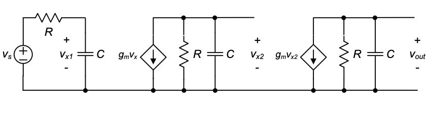
P3.14 In this chapter, we saw that using the OCT method to estimate a circuits’ bandwidth tends to be conservative. For example, in a circuit with two identical real poles (and no zeros), the bandwidth predicted using the OCT method is \(22\%\) lower than the actual bandwidth [see Equation 3.75]. Derive an analytical expression \(f(n)\) that returns the percent error of the OCT analysis for a circuit with n identical real poles and no zeros. Note that \(f(2) = –22\%\).
P3.15 Consider the common-source voltage amplifier of Figure 3.24. The goal of this design problem is to achieve a small-signal DC gain of \(-4\) and a 3-dB bandwidth of \(80\) \(MHz\). In addition, we wish to minimize the current consumption of the circuit. For simplicity in your calculations, neglect channel-length modulation and consider only the intrinsic gate capacitance. Assume the following parameters: \(R_s = 2R_D\), \(R_D\) = \(5\) \(k\Omega\), \(C_L\) = \(1\) \(pF\).
Show that the required drain current \(I_D\) is related to the circuit’s parameters and specifications as expressed below. In your analysis, approximate \(\omega_{3dB}\) using an OCT analysis. Plot \(I_D\) as a function of \(V_{OV}\) for \(L = 1\) \(\mu m\) and \(L = 1.5\) \(\mu m\).\[I_D = \frac{1}{2}\frac{ C_L \cdot |A_{v0}| \cdot \omega_{3{dB}} \cdot V_{OV}}{1 - \frac{2}{3} \frac{L^2}{\mu_n V_{OV}} \cdot \frac{R_s}{R_D} \cdot |A_{v0}| \, \omega_{3dB}}\] Note from this result that the choice of the gate overdrive voltage \(V_{OV}\) plays an important role in minimizing the required drain current.
From the expression and plots found in part (a), it is clear that the minimum channel length minimizes the current consumption of the amplifier. Explain in your words why this should be the case.
The drain current expression derived in (a) has a minimum for a certain value of \(V_{OV}\). Calculate this value assuming \(L = 1\) \(\mu m\) (minimum length). Also calculate \(R_D\), the device width and drain current for the transistor at this optimum point.
Simulate the design using SPICE with the bias current and device geometries calculated in part (c). Measure the bandwidth of the circuit using an AC simulation. Since the SPICE transistor model contains extrinsic capacitances and finite output resistance, your circuit should fall short of the desired specs (despite the fact that we have used a conservative OCT estimate for \(\omega_{3dB}\)). Calculate the percent discrepancies in the gain and bandwidth of the circuit.
Use a spreadsheet or math tool (Excel, \(MATLAB^{®*}\), etc.) to setup the design equations for gain and bandwidth that include extrinsic capacitances and finite output conductance. With these additional modeling components added, it is difficult to derive a compact closed form solution as above. However, the setup in the spreadsheet will allow you to sweep the design parameters easily to find the new optimum that meets the gain and bandwidth specs. There are many different ways in which the spreadsheet can be structured. One is to use the width of the transistor as the main “knob” and calculate/iterate over all other parameters. The hand-calculated result can be used as an initial guess in this optimization. Use your spreadsheet to calculate the new bias current and device size that will meet the specs.
Simulate the refined design from (e) in SPICE and verify that you meet the desired specs. What is the obtained \(I_D\), and how much larger is this value compared to the result from (c)?
MATLAB is a registered trademark of The MathWorks, Inc.,
3 Apple Hill Road, Natick, MA.
P3.16 For the circuit shown in Figure 3.30, prove the following results, quantifying the Thévenin resistances seen between each pair of transistor terminals. Neglect the finite \(r_o\) of the MOSFET.
\[ R_{gs} = \frac{R_G + R_S}{1 + g_m R_S} \]
\[ R_{ds} = \frac{R_D + R_S}{1 + g_m R_S} \]
\[ R_{gd} = R_G + R_D + G_m R_G R_D \]
where
\[ G_m = \frac{g_m}{1 + g_m R_S} \]
P3.17 The circuit shown in Figure 3.31 is called a “source degenerated” common-source voltage amplifier. Analyze this circuit as indicated below.
Neglecting channel-length modulation and all capacitances in the circuit, show that the circuit’s small-signal DC gain is given by \[ \frac{v_{out}}{v_{in}} \simeq -G_mR_D\] where \[G_m = \frac{g_m}{1+ g_mR_S}\] is called the compound transconductance.
Using the results stated in Problem 3.16, estimate the DC gain and 3-dB bandwidth of the circuit assuming the following parameters: \(R_G = 10\) \(k\Omega\), \(R_S\) = \(1\) \(k\Omega\), \(R_D\) = \(5\) \(k\Omega\), \(I_D\) = \(500\) \(\mu A\), \(L= 1\) \(\mu m\), and \(W= 20\) \(\mu m\). Consider only the two time constants contributed by \(C_{gs}\) and \(C{gd}\).