4 The Common-Gate and Common-Drain Stages
As we have seen from the discussion in the previous two chapters, the common-source stage can be used to realize a basic voltage amplifier. In this chapter, we will introduce the common-gate and common-drain stages, which, for instance, can be combined with the common-source amplifier to enhance its performance. More generally, as already indicated in Section 1-1, most analog amplifier circuits can be modeled as a combination of common-source, common-gate and common-drain configurations. For this reason, the three basic stage configurations can be viewed as the “atoms” of analog circuit design.
◆ Analyze the common-gate and common-drain stages with respect to their low- and high-frequency transfer functions and port resistances (and impedances).
◆ Extend the MOSFET model as needed to capture relevant new effects that must be included in the analysis.
◆ Provide a first pass look at application examples for the common-gate and common-drain stages
4.1 Overview of Stage Configurations
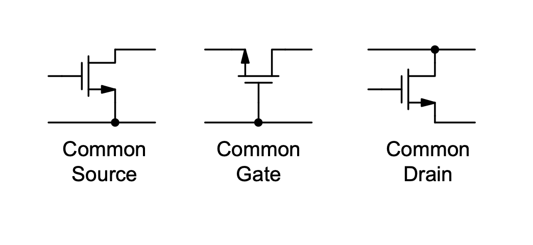
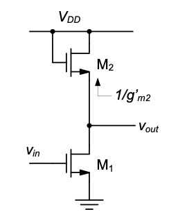
In the common-source (CS) amplifier discussed in the previous chapters, the input signal is applied to the gate and the output signal is taken from the drain. In a common-gate (CG) amplifier, the source is used as the input and the drain serves as the output terminal. In the common-drain (CD) amplifier, the input is applied at the gate and the output is taken from the source. Thus, in the context of two-port amplifiers with one terminal common between the input and output, the CS, CG, and CD circuits represent all three possible configurations (see Figure 4.1).
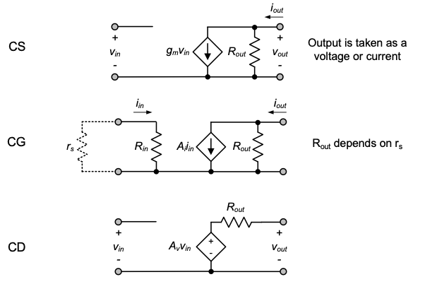
In our detailed analysis of the CG amplifier, we will find that this topology has a very low input resistance and a very high output resistance, which is exactly what we would want in a current amplifier. Conversely, the CD stage has a high input resistance and a small output resistance, which corresponds to the desired characteristics of a voltage amplifier (see Section 1-3).
4.2 Bulk Connection Scenarios and Required Model Extensions
Before engaging in a detailed analysis of the CG and CD stages, we need to think about the bulk connection in these stages. For the CS stage discussed so far, it was natural to connect the bulk to the source of the MOSFET. However, now that the source is connected either to the input or output port, we need to develop an understanding of the available options.
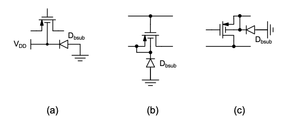
The first aspect to consider is related to technology constraints, and specifically how the n-channel and p-channel devices are formed in the integrated circuit substrate. As already indicated in Section 2-1-2, we assume in this module that the MOSFETs are built in a so-called n-well technology (see Figure 4.2). This means that the substrate is p-type, and the n-channel transistors are formed directly in the substrate. In order to create p-channels, n-type wells are diffused into the substrate, and the p-channels are subsequently formed in these regions.
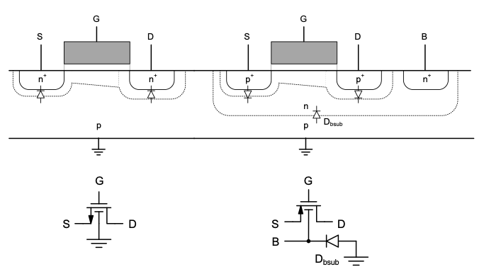
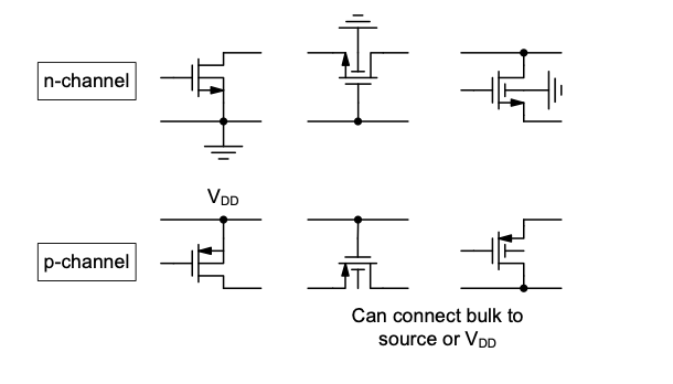
Given the cross-section of Figure 4.2, it is clear that all n-channel transistors share the same bulk node. In contrast, the bulk node of a p-channel MOSFET can be isolated and freely connected to an arbitrary potential. Figure 4.3 shows the possible bulk connection scenarios arising from these constraints. For CG and CD stages built using n-channels in an n-well process, the bulks are always connected to the substrate potential (assumed to be “ground” in this module) by default. On the other hand, we are free to choose the bulk connection in p-channel CG and CD amplifiers. The most common scenarios encountered in practice are to tie the p-channel bulk to the supply voltage (\(V_{DD}\)), or to the source terminal. Either choice can have advantages and disadvantages, depending on the given circuit. In order to be able to reason about the associated tradeoffs, we will now extend the MOSFET model such that the bulk node is incorporated as a fourth “free” terminal.
4.2.1 Well Capacitance
As indicated in Figure 4.2, the n-well region of the p-channel transistor forms a pn-junction with the p-type substrate (\(D_{bsub}\)). Similar to the junctions formed by the source/drain regions (see Section 3-3-1), we can model this junction as a parasitic capacitance between the bulk terminal and the substrate. Whether or not this capacitance must be considered depends on the bulk connection. As shown in Figure 4.4, if the bulk is tied to the supply, the junction capacitance is typically irrelevant, since it is connected between \(V_{DD}\) and ground, having no impact on circuit nodes that carry the signal. On the other hand, if the bulk is connected to the source, the capacitance will appear across the input port for the CG stage, and across the output port of the CD stage. In this case, the parasitic capacitance contribution from the well must be taken into account.
Similar to the expression we used to estimate the source/drain junction capacitances, we can obtain an estimate for the well capacitance using
\[ C_{bsub} = \frac{C_{Jwell \cdot A_{well}}}{(1+V_{BSUB} / PB)^{MJ}} \tag{4.1}\]
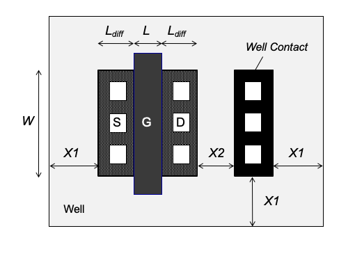
This expression is similar to Equation 3.33, except that the sidewall contribution has been omitted for simplicity. In Equation 4.1, \(V_{BSUB}\) is the voltage between the bulk node and the substrate (a positive voltage, i.e.,the junction is reverse biased). \(C_{Jwell}\) is the zero-bias depletion capacitance parameter for the junction and Awell is the area of the n-well under consideration. The well area depends strongly on the actual layout of the transistor. However, for approximate calculations it is often sufficient to assume a basic rectangular well shape using reasonable geometry estimates. We will illustrate this using an example.
Example 4-1: Well Capacitance Calculation
Consider a p-channel MOSFET that was laid out as shown in Figure 4.6. Estimate the well-to-substrate capacitance Cbsub assuming the following parameters: \(W = 10\) \(μm\), \(L = 3\) \(μm\), \(X_1 = 5\) \(μm\) (diffuion to well edge spacing), \(X2 = 3\) \(μm\) (diffusion spacing), \(C_{Jwell} = 0.05\) \(fF/μm^2\), and \(V_{BSUB} = 2.5\) \(V\).
SOLUTION
From Figure 4.6, we see that
\[ A_{welll} = (W + 2X_1) \cdot (L +3L_{diff} + 2X_1 +X_2) \]
\[ = (10 +10) \cdot (1 + 6 + 10+ 3)µm^2 \]
\[ = 400µm^2 \]
Using Equation 4.1 and the technology parameters for \(PB\) and \(MJ\) from Table 3-1, we obtain
\[ C_{bsub} = \frac{C_{Jwell \cdot A_{well}}}{(1+V_{BSUB} / PB)^{MJ}} \]
\[ = \frac{0.05fF \cdot400}{(1+2.5 / 0.95)^{0.95}} \]
\[ = 10.5fF \]
From the above calculation, we see that the well capacitance can be comparable to the intrinsic and extrinsic device capacitances (see Example 3-5). Hence, whenever the designer chooses a bulk connection for which the well capacitance appears at an internal circuit node (other than the supply), care must be taken in estimating \(C_{bsub}\) and incorporating this capacitance in the overall circuit model.
As a final note, it is worth mentioning that most circuit simulation tools, such as SPICE, do not automatically account for the well capacitance. Whenever relevant, the circuit designer must (manually) ensure that an appropriate modeling element is included in the simulation. This can be done, for example, by adding a properly modeled diode or capacitor to the node in question.
4.2.2 Backgate Effect
In Section 2-1, we analyzed the MOSFET’s I-V characteristics assuming that the bulk node is connected to the source, i.e., \(V_{SB}\) = 0. However, in the CG and CD configurations, this is not the case unless the designer opted for a source-to-bulk tie as in the circuits of Figure 4.4(b) and (c). Therefore, we will now refine the I-V expressions from Section 2-1, for the case of non-zero \(V_{SB}\) and using an n-channel MOSFET for the analysis.
For an n-channel device with positive \(V_{SB}\) — i.e., the source lies at a higher potential than the (grounded) substrate — the primary effect is that the depletion region between the source and the substrate is widened (see Figure 4.7). This follows from the usual behavior of pn junctions — the depletion region of a reverse biased junction widens for increasing reverse bias.
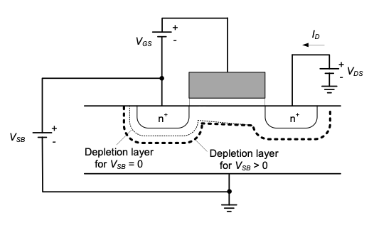
Qualitatively speaking, the widened depletion region increases the amount of negative fixed charge (\(NA^-\)) near the source. This extra negative charge opposes the injection of electrons from the source, and hence a larger \(V_{GS}\) is needed to cause the same drain current \(I_D\). The larger required \(V_{GS}\) is commonly modeled as an effective increase in the device’s threshold voltage. The dependence of the threshold voltage on the bulk-source voltage is called backgate effect. A detailed analysis based on solid-state physics reveals that the relationship between the applied \(V_{SB}\) and the MOSFET’s threshold voltage is given by the following expression (see Reference 1):
\[ V_{Tn}(V_{SB}) = V_{TOn} + γ_n(\sqrt{2φ_f+V_{SB}}-\sqrt{2φ_f}) \tag{4.2}\]
where \(V_{TOn}\) is the threshold voltage without backgate effect, \(γ_n\) is the n-channel MOSFET backgate effect parameter, and \(φ_f\) is the surface potential parameter. With backgate effect included, the large-signal I-V characteristic for the saturation region is
\[ I_D = \frac{1}{2} \mu_n C_{ox} \frac{W}{L} ({V_{GS}} - V_{Tn}(V_{SB}))^2 (1+\lambda_n V_{DS}) \tag{4.3}\]
which is identical to Equation 2.45, except that \(V_{Tn}\) is now a function of \(V_{SB}\), as defined in Equation 4.2.
In order to incorporate the backgate effect into the small signal model of the transistor, we will follow exactly the same approach as in Section 2-3-1. That is, we approximate the incremental drain current around the operating point as the total differential, now with a drain current perturbation due to \(v_{bs}\) included:
\[ i_d = \left.\frac{\partial i_D}{\partial v_{GS}}\right|_{Q}\, v_{gs} + \left.\frac{\partial i_D}{\partial v_{DS}}\right|_{Q}\, v_{ds} + \left.\frac{\partial i_D}{\partial v_{BS}}\right|_{Q}\, v_{bs} \tag{4.4}\]
\[ = g_mv_{gs} + g_ov_{ds} + g_{mb}v_{bs} \]
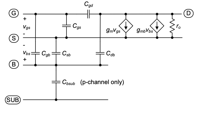
In this expression, gm and go are the transconductance and output conductance, respectively, and as derived previously in Chapter 2. The new term \(g_{mb}\) is called backgate transconductance and represents the perturbation of the drain current by an incremental change in the bulk-source voltage.
To compute \(g_{mb}\), it is convenient to expand the partial derivative in Equation 4.4 using the chain rule
\[ g_{mb} = \left.\frac{\partial i_D}{\partial v_{BS}}\right|_{Q} \]
\[ = \left.\frac{\partial i_D}{\partial (V_{GS} - V_{Tn})}\right|_{Q} \left.\frac{\partial (V_{GS} - V_{Tn})}{\partial V_{Tn}}\right|_{Q} \left.\frac{\partial V_{Tn}}{\partial v_{BS}}\right|_{Q} \tag{4.5}\]
The first partial derivative in the above expression is simply \(g_m\). The second term is equal to –1. Therefore, after partial differentiation of the threshold voltage Equation 4.2 we obtain
\[ g_{mb} = -g_m \left.\frac{\partial V_{Tn}}{\partial v_{BS}}\right|_{Q} = \frac{g_m \gamma_n}{2\sqrt{2\phi_f + V_{SB}}} \tag{4.6}\]
Analogous to the way we incorporated \(g_m\) and \(g_o\), the backgate transconductance can be included in the transistor’s small signal model as shown in Figure 4.8. As defined in Equation 4.4, the \(g_{mb}\) element captures the dependence of the drain current to incremental changes in the bulk-source voltage. From this final result, we see that the term backgate was coined to reflect that the bulk acts just like another gate of the transistor. The only difference between the backgate and the actual gate node is that the backgate is physical located at the back side of the MOSFET, separated from the channel by a depletion layer.
For circuit design, it is useful to have a feel for the magnitude of \(g_{mb}\), as well as for the range of threshold voltage ranges for typical bias conditions. The following example investigates typical numbers for the technology assumed in this module.
Example 4-2 {#example-4-2}: Backgate Effect
Consider an n-channel MOSFET with the following parameters \(V_{T0n} = 0.5\ \mathrm{V}\), \(\gamma_{n} = 0.6\ \mathrm{V^{1/2}}\), \(\phi_{f} = 0.4\ \mathrm{V}\), and \(V_{SB} = 2.5\ \mathrm{V}\), \(1.5\ \mathrm{V}\), and \(0\ \mathrm{V}\).
For each case, calculate \(V_{Tn}\) and the ratio \(\frac{g_{mb}}{g_{m}}\).
SOLUTION
Evaluating Eqs. (4.2) and (4.6) for \(V_{SB} = 2.5\ \mathrm{V}\), we have
\[ V_{Tn} = V_{TOn} + \gamma_n \left( \sqrt{2\phi_f + V_{SB}} - \sqrt{2\phi_f} \right) \]
\[ = 0.5\ \mathrm{V} + 0.6\ \mathrm{V^{1/2}} \left( \sqrt{0.8\ \mathrm{V} + 2.5\ \mathrm{V}} - \sqrt{0.8\ \mathrm{V}} \right) = 1.05\ \mathrm{V} \]
\[ \frac{g_{mb}}{g_m} = \frac{\gamma_n}{2\sqrt{2\phi_f + V_{SB}}} = \frac{0.6\ \mathrm{V^{1/2}}}{2\sqrt{0.8\ \mathrm{V} + 2.5\ \mathrm{V}}} = 0.165 \]
After evaluating the same expressions for the remaining two cases, we can summarize the obtained results as shown in the table below.
| \(V_{SB}\) [V] | \(V_{Tn}\) [V] | \(g_{mb} / g_m\) |
|---|---|---|
| 2.5 | 1.05 | 0.165 |
| 1.5 | 0.87 | 0.198 |
| 0 | 0.50 | 0.335 |
From these values, we see that the threshold voltage of an n-channel MOSFET in our technology shifts up by about \(0.5 V\) as the source-bulk bias voltage approaches \(2.5 V\) (half of the supply voltage assumed in this module). The backgate transconductance ranges approximately between 15% and 30% of gm over the same backgate bias range. Note that the backgate transconductance reduces for larger \(V_{SB}\). This makes intuitive sense, since the depletion region widens for larger reverse bias. Qualitatively speaking, this increases the distance from the bulk electrode to the inversion layer, weakening the effect of backgate voltage changes on the incremental drain current.
Table 4-1 summarizes the MOSFET modeling parameters for our standard technology with backgate effect parameters included. This table represents the complete set of parameters used in this module; no further extensions will be needed.
| Parameter | n-channel MOSFET | p-channel MOSFET |
|---|---|---|
| Threshold voltage | \(V_{Tn}\) = 0.5V | \(V_{Tp}\) = -0.5V |
| Transconductance parameter | \(μ_nC_{ox}= 50μA/V^2\) | \(μ_pC_{ox}= 25μA/V^2\) |
| Chanel length modulation parameter | \(\lambda_n =0.1V^{-1}/L\) (\(L\) in \(\mu m\)) |
\(\lambda_p =0.1V^{-1}/L\) (\(L\) in \(\mu m\)) |
| Gate oxide capacitance per unit area | \(C_{ox} = 2.3fF/\mu m^2\) | |
| Overlap Capacitance | \(C_{ov} = 0.5fF/\mu m\) | |
| Zero-bias planar bulk depletion capacitance | \(C_{Jn} = 0.1fF/\mu m^2\) | \(C_{Jp} = 0.3fF/\mu m^2\) |
| Zero-bias sidewall bulk depletion capacitance | \(C_{JSWn}=0.5fF/\mu m\) | \(C_{JSWp}=0.35fF/\mu m\) |
| Bulk junction potential | \(PB = 0.95\) \(V\) | |
| Planar bulk junction grading coefficient | \(MJ = 0.5\) | |
| Sidewall bulk junction grading coefficient | \(MJSW = 0.33\) | |
| Length of source and drain diffusions | \(L_{diff} = 3\mu m\) | |
| Backgate effect parameter | \(\gamma_n\) = \(0.6^{\frac{1}{2}}\) | \(\gamma_n\) = \(0.6^{\frac{1}{2}}\) |
| Surface potential parameter | \(\phi_f = 0.4V\) | |
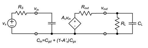
4.3 Analysis of the Common-Gate Stage
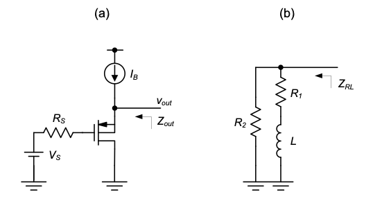
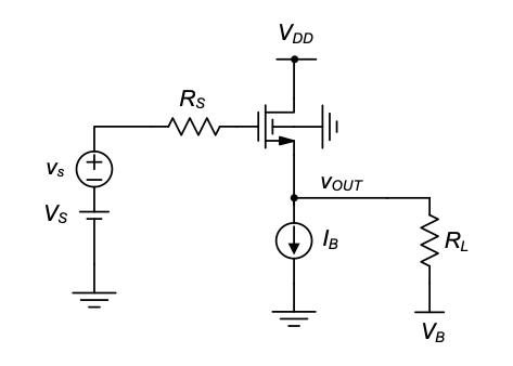
Using the additional modeling insight obtained in the previous section, we are now ready to analyze the CG circuit in detail. For the derivations in this section, we will assume the circuit topology shown in Figure 4.1. In this example configuration, the MOSFET’s quiescent point drain current (and \(V_{GS}\)) is established using the input bias current source \(I_B\). The auxiliary bias voltage source \(V_B\) is used to define the operating point node voltages at the gate and source of the transistor. The resistor \(R_D\) sources the bias current and sets the quiescent point voltage at the output node. One minor additional point to note is that the circuit is drawn different from Figure 4.1(b) such that the drain node lies above the source. This is the preferred way to draw this circuit for large-signal analysis, since one can better visualize the DC bias point levels. The drain lies at a higher DC potential than the source.
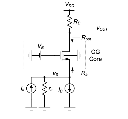
Since there are many different ways to configure the source, bias, and load network of the stage, we distinguish the circuitry outside the dashed line from the core of the stage, which is essentially just the MOSFET with its ac-grounded gate. This distinction makes the results derived below more modular and generally applicable. For instance, when we derive expressions for small-signal port resistances, we distinguish between the core components (\(R_{in}\) and \(R_{out}\) shown in Figure 4.9) and any resistances in the source, bias, and load network that appear in parallel. Also, depending on how the CG circuit is used, the output variable of interest may be either the voltage at the output or the current that flows into the output network. For the discussion in this chapter, we assume that the intended output is the voltage \(v_{OUT}\) as indicated in Figure 4.9. With this choice, the (low-frequency) gain of the circuit \(v_{out}/i_s\) is a transresistance.
The detailed analysis below consists of several parts. First, we will establish basic expressions for the circuit’s operating point and derive the conditions for MOSFET operation in the saturation region. Next, we will analyze the CG circuit core in terms of its port resistances, which will show that it is most appropriately modeled as a current amplifier. Finally, the obtained results are extended to include high-frequency effects due to capacitive elements.
4.3.1 Bias Point Analysis
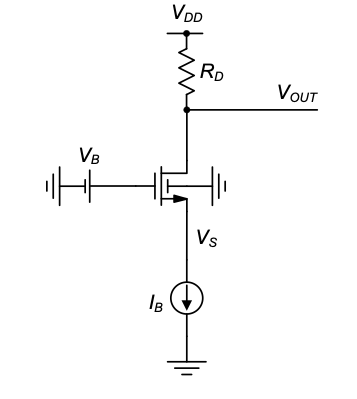
To determine the amplifier’s node voltages at the operating point, we consider the circuit with the small-signal source \(i_s\) and its (small-signal) source resistance \(r_s\) removed (see Figure 4.10). From this circuit we see that \(I_D\) = \(I_B\), and thus
\[ V_{OUT} = V_{DD} - I_B R_D \tag{4.7}\]
A more complex analysis is needed to find the voltage at the source node, \(V_S\).
We begin by recognizing that
\[ V_S = V_B - V_{GS} \tag{4.8}\]
Assuming that the MOSFET operates in the saturation region (which is subject to verification), we know that
\[ I_D = I_B = \frac{1}{2} \mu_n C_{ox} \frac{W}{L} (V_{GS} - V_{Tn})^2 (1 + \lambda_n V_{DS}) \tag{4.9}\]
where
\[ V_{Tn} = V_{TOn} + \gamma_n \left( \sqrt{2\phi_f + V_{SB}} - \sqrt{2\phi_f} \right) \tag{4.10}\]
and \(V_{SB} = V_S\). Neglecting channel length modulation (i.e., assuming \(\lambda_n V_{DS} ≅ 0\)), we can solve Equation 4.9 for \(V_{GS}\):
\[ V_{GS} = V_{Tn} + \sqrt{\frac{I_B}{\frac{1}{2} \mu_n C_{ox} \frac{W}{L}}} = V_{Tn} + V_{OV} \tag{4.11}\]
Substituting back into Equation 4.8, we have
\[ V_S = V_B - V_{Tn}(V_S) - \sqrt{\frac{I_B}{\frac{1}{2} \mu_n C_{ox} \frac{W}{L}}} \tag{4.12}\]
Unfortunately this is a transcendental equation and obtaining a precise solution will require numerical iterations (using Equation 4.10 with \(V_{SB}\) = \(V_S\)). However, since the dependence of \(V_{Tn}\) on \(V_S\) is relatively weak, a calculation with one or two iterations tends to give a satisfactory answer for the purpose of hand analysis. This is illustrated in Example 4.3 below. Once \(V_S\) is computed, we can ensure that the MOSFET operates in saturation by checking the following inequality:
\[ V_{DS} = V_{OUT} - V_{S} > V_{DSsat} = V_{GS} - V_{Tn} \tag{4.13}\]
Example 4-3: Well Bias Point Calculation for a Common Gate Stage
Consider the common-gate circuit shown in Figure 4.10 with the following parameters: \(V_{DD} = 5\ \mathrm{V}\), \(V_{B} = 2.5\ \mathrm{V}\), \(I_{B} = 400\ \mu\mathrm{A}\), \(R_{D} = 3\ \mathrm{k\Omega}\).
For the MOSFET, assume \(W = 100\ \mu\mathrm{m}\), \(L = 1\ \mu\mathrm{m}\), and the standard technology parameters given in Table 4-1.
Compute \(V_{OUT}\), \(V_S\), as well as \(V_{DS}\) and \(V_{OV} = V_{GS} - V_{Tn}\) of the transistor.
SOLUTION
Using Equation 4.7 we can directly compute
\[ V_{OUT} = V_{DD} - I_B R_D = 5\ \mathrm{V} - 1.2\ \mathrm{V} = 3.8\ \mathrm{V} \]
Next, we find
\[ V_{GS} - V_{Tn} = \sqrt{\frac{I_B}{\frac{1}{2} \mu_n C_{ox} \frac{W}{L}}} = 0.4\ \mathrm{V} \]
In order to determine \(V_S\), we begin by first ignoring the backgate effect, i.e., the evaluation of Equation 4.12 using the given numbers
\[ g_{mb} = \left.\frac{\partial i_D}{\partial v_{SB}}\right|_{Q} = \left.\frac{\partial i_D}{\partial (V_{GS} - V_{Tn})}\right|_{Q} \left.\frac{\partial (V_{GS} - V_{Tn})}{\partial V_{Tn}}\right|_{Q} \left.\frac{\partial V_{Tn}}{\partial v_{BS}}\right|_{Q} \]
Using this estimate of \(V_S\), we can now compute an estimate of the actual threshold voltage with backgate effect included.
By evaluatin Equation 4.10, we find
\[ V_{Tn} = \left( 0.5\ \mathrm{V} + 0.6\ \mathrm{V}^{1/2} \left( \sqrt{0.8\ \mathrm{V} + 1.6\ \mathrm{V}} - \sqrt{0.8\ \mathrm{V}} \right) \right) = 0.893\ \mathrm{V} \]
and thus
\[ V_S = 2.5\ \mathrm{V} - 0.893\ \mathrm{V} - 0.4\ \mathrm{V} = 1.207\ \mathrm{V} \]
This result for \(V_S\), which was obtained using only one iteration, differs from the exact solution \(V_S = 1.273\ \mathrm{V}\) (obtained through computer simulations or further iterations) by only \(-67\ \mathrm{mV}\) (\(-5.2\%\)).
With the above numbers, we have \[ V_{DS} = V_{OUT} - V_{S} = 3.8\ \mathrm{V} - 1.207\ \mathrm{V} = 2.59\ \mathrm{V} > V_{GS} - V_{Tn} = 0.4\ \mathrm{V} \]
Therefore, the transistor indeed operates in the saturation region, as assumed initially.
4.3.2 First Pass Low-Frequency Analysis
In order to establish symbolic expressions for the stage’s small-signal transfer characteristics, we will first ignore capacitive elements and focus on the low-frequency behavior. Based on the circuit of Figure 4.9, we can thus construct the low-frequency small-signal model shown in Figure 4.11. Note here that, as already explained in Chapter 2, the DC bias current source was removed, and the DC voltage sources were replaced by a connection to ground.
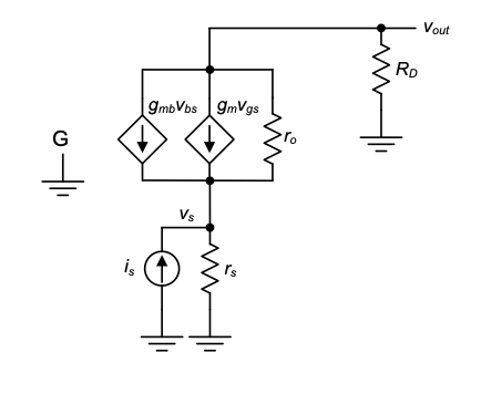
In principle, we could use the circuit of Figure 4.11 directly to carry out a detailed analysis. However, it is beneficial to first walk through a few circuit simplifications that reduce the algebraic effort and also provide qualitative insight. First, note that since the gate and the bulk of the MOSFET are small-signal grounds, it follows that \(v_{gs} = -v_s\) and \(v_{bs} = -v_s\). Thus, the current generators \(g_m\) and \(g_{mb}\) effectively add, since they are controlled by the same voltage (\(-v_s\)). For notational convenience, we therefore define
\[ g' = g_m + g_{mb}. \]
The resulting circuit is shown in Figure 4.12(a) (with the controlled source rotated for convenience).
As a next step, we split the controlled current source into two elements as depicted in Figure 4.12(b). Since this change does not alter the summation of currents at the two nodes, the obtained circuit is equivalent to that of Figure 4.12(a). Next, we recognize that the controlled source on the left side is simply a resistor with value \(\frac{1}{g'_m}\). This is true because for this element we have
\[ i = g'_m\, v \quad \Longrightarrow \quad R = \frac{v}{i} = \frac{1}{g'_m}. \]
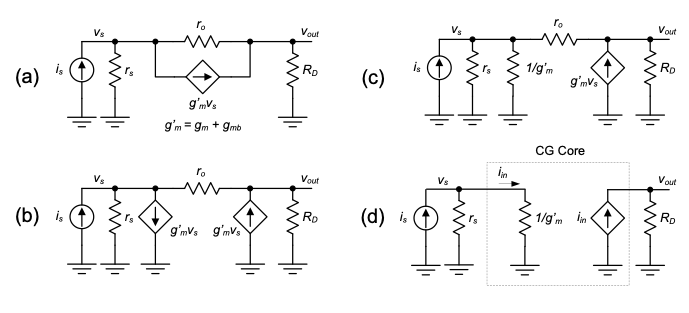
In the resulting circuit of@fig-4.10(c), let us assume for the time being that the resistance ro has negligible impact on the operation of the CG amplifier. In this case, shown in Figure 4.12(d), the core of the CG stage perfectly conforms with the unilateral current amplifier two-port model discussed in Section 1-3. Specifically, note that the circuit has low input resistance (for example, if \(g'm = 10mS => \frac{1}{g'm} = 100 \ohm\)) and high output resistance (\(R_{out}\) → \(\infty\)), as desired for a current amplifier. The current gain (\(A_i\)) of the two-port is equal to one; any current that enters the core part of the CG stage passes through it unchanged. This result makes intuitive sense also from the original circuit in Figure 4.9. Any change in the MOSFET’s source current must also appear at the drain side.
A secondary conclusion to draw from this first-pass analysis concerns the backgate connection of the transistor. If the bulk terminal were not connected to ground, but instead tied to the source of the transistor (which is possible for the p-channel version of the circuit in our n-well technology), we would have \(v_{bs} = 0\), and the \(g'm\) term would reduce to \(g_m\). This is undesired since the amplifier’s input resistance will increase correspondingly (on the order of 15–35%, see Example 4-2). Thus, in a CG amplifier, it is typically advantageous to leave the bulk node ac-grounded, rather than tying it to the source. Note that this also reduces the parasitic capacitance at the source, as discussed in Section 4-2-1.
4.3.3 Detailed Low-Frequency Analysis
We will now carry out a more detailed analysis that refines the result obtained in the previous subsection. Specifically, we wish to perform a full analysis with the MOSFET’s ro included to see if, and precisely when, this resistor can be neglected.
We begin by computing the input resistance (\(R_{in}\)) of the CG circuit core using the full circuit from Figure 4.12(c), redrawn in Figure 4.13(a) with a test voltage source included. From this setup, the input resistance is found using the procedure described in Section 1-3-3. Specifically, note that \(R_D\) is included in the analysis since the circuit is bilateral.
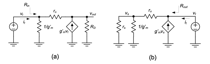
Now, writing KVL at the input and output nodes gives
\[ i_t = g'_m v_t + \frac{v_t - v_{out}}{r_o} \tag{4.14}\]
\[ 0 = -g'_m v_t - \frac{v_t - v_{out}}{r_o} + \frac{v_{out}}{R_D} \tag{4.15}\]
By solving this system of equations for \(v_t\) and \(i_t\), we obtain
\[ R_{in} = \frac{v_t}{i_t} = \frac{1 + \frac{R_D}{r_o}}{g'_m + \frac{1}{r_o}} \tag{4.16}\]
Assuming \(r_o \gg R_D\) and \(r_o \gg 1/g'_m\), the input resistance becomes approximately
\[ R_{in} ≅ \frac{1}{g'_m} \tag{4.17}\]
which is identical to the value postulated in the approximate model of the previous subsection. The approximation applied to the denominator of Equation 4.16 is always valid, since \(g'_m r_o \gg 1\) for a typical MOSFET. The approximation made in the numerator may not hold when the drain is terminated with a very large incremental resistance, as, for instance, found in a current source. In this case, care must be taken to use the exact numerator of Equation 4.16.
Next, to calculate the output resistance (\(R_{out}\)), we set the small-signal input current source is equal to zero (open circuit) but leave the effect of its source resistance (\(r_s\)) in place as shown in Figure 4.13(b). As before, we place a test voltage source at the port of interest, and write KCL for the two nodes of the circuit.
\[ 0 = g'_m v_s + \frac{v_s - v_{out}}{r_o} + \frac{v_s}{r_s} \tag{4.18}\]
\[ i_t = -g'_m v_s - \frac{v_s - v_{out}}{r_o} \tag{4.19}\]
After solving for \(v_t\) and \(i_t\), we obtain
\[ R_{out} = \frac{v_t}{i_t} = r_o + r_s \left[ 1 + g'_m r_o \right] \tag{4.20}\]
Utilizing the fact that \(g'_m r_o \gg 1\), we can approximate
\[ R_{out} ≅ r_o \left[ 1 + g'_m r_s \right] \tag{4.21}\]
Under the condition that \(g'_m r_s \gg 1\), the expression further simplifies to
\[ R_{out} ≅ g'_m r_o r_s \tag{4.22}\]
From this result, we note that the source resistance \(r_s\) is multiplied by a term that is on the order of the intrinsic voltage gain of the transistor (\(g_mr_o\)), which is typically greater than 100 in our technology (see Section 2-3-2). Thus, a CG stage can essentially be used to turn a current source with moderate source resistance (\(r_s\)) into a “better” current source with very high source resistance. This feature is widely used in a variety of circuit configurations, some of which will be discussed later in this module.
Using the above results, we can now construct a complete circuit model that includes the CG core as a unilateral current amplifier two-port (see Figure 4.14). Using this model, the transresistance gain from the input current source (\(i_s\)) to the circuit’s output voltage (\(v_{out}\)) can be written as
\[ \frac{v_{out}}{i_s} = \frac{i_{in}}{i_s} \cdot \frac{v_{out}}{i_{in}} = \frac{r_s}{r_s + R_{in}} \cdot \left( \frac{1}{R_D} + \frac{1}{R_{out}} \right)^{-1} \tag{4.23}\]
where the first term represents the current divider formed by \(r_s\) and \(R_{in}\) and the second term is the parallel combination of \(R_D\) and \(R_{out}\).
For a typical application of this circuit, where \(R_{in} \ll r_s\) and \(R_D \ll R_{out}\), Equation 4.23 simplifies to
\[ \frac{v_{out}}{i_s} \equiv R_D \tag{4.24}\]
In words, the transresistance of the circuit is approximately equal to the drain resistance. This makes intuitive sense since the CG core acts a current amplifier with a gain near unity. That is, the CG stage absorbs all (or most) of the current from the input source, and it passes this current to the termination resistance (\(R_D\)), causing a proportional change in the output voltage.
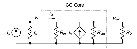
When employing the model of Figure 4.14, it is important to remember that we are approximating a bilateral circuit using a unilateral model. We have investigated the resulting error for this particular configuration in Example 1-3 and found that the unilateral model is guaranteed to be accurate as long as the coupling resistance between the input and output ports (\(R_2\) in Example 1-3 and \(r_o\) in the analyzed CG circuit) is larger than the termination resistance (\(R_L\) in Example 1-3 and \(R_D\) in the analyzed CG circuit). Thus, the result stated in Equation 4.23 holds with good accuracy as long as \(R_D \ll r_o\), a condition that is satisfied in many relevant applications.
4.3.4 High-Frequency Analysis
In order to model the frequency response of the CG amplifier, we now include the capacitances of the MOSFET into the small-signal model constructed in the previous section (see Figure 4.15).
Since both the gate and bulk of the MOSFET are AC-grounded, \(C_{gs}\) and C_{sb}$, as well as \(C_{gd}\) and \(C_{db}\) appear from source and drain, respectively, to ground. For notational convenience, we abbreviate \(C_{gs} + C_{sb} = C_s\) and \(C_{gd} + C_{db} = C_d\) in the following treatment.
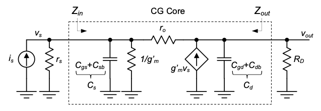
One way to analyze the circuit of Figure 4.15 is to reuse the results obtained in the low-frequency analysis, but now with \(C_s\) and \(C_d\) added in parallel to \(r_s\) and \(R_D\), respectively. In this spirit, we begin by considering the effect of the added capacitances on the circuit’s input impedance, \(Z_{in}\). Reusing the result from Equation 4.16, we can write
\[ Z_{in} ≅ \frac{1 + \frac{R_D \parallel \frac{1}{s C_d}}{r_o}}{g'_m} \ \Big\| \ \frac{1}{s C_s} \tag{4.25}\]
As long as \(R_D \ll r_o\), regardless of the added term due to \(C_d\), the numerator can be approximated as unity. Therefore, it follows that
\[ Z_{in} ≅ \frac{1}{g'_m} \ \Big\| \ \frac{1}{s C_s} \tag{4.26}\]
In other words, this result simply says that \(Z_{in}\) is typically well approximated by the parallel impedance connection of \(1 / g'_m\) and \(C_s\).
Finding the (exact) output impedance (\(Z_{out}\)) proves algebraically more difficult. However, provided that \(g'_m r_s \gg 1\) and for frequencies below the MOSFET’s cutoff frequency \(\omega_T\), it follows that (see Problem P4.6)
\[ Z_{out} \equiv g'_m r_o r_s \ \Big\| \ \frac{g'_m r_o}{s C_s} \ \Big\| \ \frac{1}{s C_d} \tag{4.27}\]
Thus, \(Z_{out}\) consists of the parallel combination of:
(1) \(r_s\), increased by the factor \(g'_m r_o\) (this is simply \(R_{out}\) from the low-frequency analysis),
(2) the explicit capacitance present at the output (\(C_d\)), and
(3) the reactance of the source side capacitance (\(C_s\)) increased by the factor \(g'_m r_o\).
From the second term, we see that the MOSFET not only boosts the resistance of \(r_s\) seen from the output, but also the reactance of \(C_s\). Since usually \(C_s / g'_m r_o \ll C_d\), we can safely neglect the second term of@eq-4.27 and conclude
\[ Z_{out} \equiv g'_m r_o r_s \ \Big\| \ \frac{1}{s C_d} \tag{4.28}\]
In summary, the overall conclusion is that, to first order, the drain and source side capacitances can simply be added to the ports of the already obtained low-frequency model of Figure 4.14. Thus, we have once again arrived at a relatively simple unilateral model for the circuit that holds for high frequencies. The corresponding circuit model is drawn out in Figure 4.14, incorporating the assumptions \(g'_m r_s \gg 1\) and \(R_D \ll r_o\).
Also, for generality, we have included a load capacitor (\(C_L\)) and a load resistor. (\(R_L\)). Note that whenever \(R_L\) carries a DC current, this resistor must also be included in the bias point calculations of the circuit.
Similar to the low-frequency analysis of the previous subsection, the overall transfer function of the circuit in Figure 4.16 is found by considering the current division at the input node, and the parallel impedance at the output node:
\[ \frac{v_{out}}{i_s} = \frac{i_{in}}{i_s} \cdot \frac{v_{out}}{i_{in}} \]
\[ = \frac{g'_m}{g'_m + s C_s} \cdot \left( \frac{1}{R_D} + \frac{1}{R_L} + s C_d + s C_L \right)^{-1} \]
\[ = [R_D \parallel R_L] \cdot \frac{1}{1 + s \frac{C_s}{g'_m}} \cdot \frac{1}{\left( [R_D \parallel R_L][C_d + C_L] \right)} \]
\[ = [R_D \parallel R_L] \cdot \frac{1}{1 - \frac{s}{p_1}} \cdot \frac{1}{1 - \frac{s}{p_2}} \tag{4.29}\]
In this expression, the leading term \([R_D \parallel R_L]\) corresponds to the low-frequency transresistance and \(p_1 = -g'_m / C_s\) and \(p_2 = -1 / \left[ (R_D \parallel R_L)(C_d + C_L) \right]\)
are the poles of the circuit.
The pole \(p_1\) is associated with the input of the circuit and captures the frequency dependence of the current transfer from the input current to the drain current of the transistor (\(i_x / i_{in}\) in Figure 4.16). The corresponding pole frequency \(g'_m / C_s\) is very close to \(\omega_T\) (the cutoff frequency of the transistor) and will rarely limit the bandwidth of the overall circuit. The pole \(p_2\) depends on the component values in the load network. If the added \(C-L\) is small, this pole will typically also lie at a very high frequency.
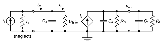
From the result of Equation 4.29, it is important to note that the circuit has two distinct and conveniently isolated poles that are not “entangled,” as for instance in the frequency response of the CS stage [see Equation 3.38]. This is a direct result of the fact that the input and output networks of the model in Figure 3.17 are decoupled, i.e., the networks that define the time constants on each side of the circuit do not interact. Note also that for approximate 3-dB bandwidth calculations, the method of open-circuit time constants can be applied. This will give the sum of the two time constants that make up the poles contained in Equation 4.29.
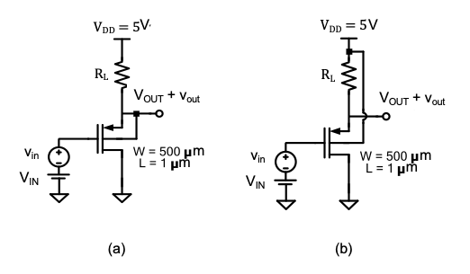
Example 4-4: Bandwidth Calculation for a Common-Gate Stage
Consider the CG circuit of Figure 4.9 using the same parameters used in Example 4-3: \(I_B = 400\ \mu\mathrm{A}\), \(R_D = 3\ \mathrm {k\Omega}\), \(W = 100\ \mu\mathrm{m}\), and \(L = 1\ \mu\mathrm{m}\). Using he bias point information from Example 4-3, compute all device capacitances and estimate the bandwidth of the circuit’s transfer function using the method of open-circuit time constants.
SOLUTION
From Example 4-3, we know that \(V_{OUT} = 3.8\ \mathrm{V}\) and \(V_S = 1.273\ \mathrm{V}\). Using Equation 3.15 and Equation 3.32-Equation 3.34 we can therefore compute all device capacitances.
\[ C_{gs} = \frac{2}{3}\,(100 \cdot 1\,\mu\mathrm{m}^2)\!\left(2.3\,\frac{\mathrm{fF}}{\mu\mathrm{m}^2}\right) + 100\,\mu\mathrm{m}\!\left(0.5\,\frac{\mathrm{fF}}{\mu\mathrm{m}}\right) = 203.3\,\mathrm{fF} \]
\[ C_{gd} = 100\,\mu\mathrm{m}\!\left(0.5\,\frac{\mathrm{fF}}{\mu\mathrm{m}}\right) = 50\,\mathrm{fF} \]
Evaluating Equation 3.34, using the source junction bias voltage of \(V_{SB} = 1.273\ \mathrm{V}\) yields
\[ C_{sb} = 19.6\,\mathrm{fF} \]
The drain junction has a reverse bias voltage of \(V_{DB} = V_{OUT} = 3.8\ \mathrm{V}\).
Evaluating Eq. (3.33) with this value and the given parameters gives
\[ C_{db} = 13.4\,\mathrm{fF} \]
The total capacitances for the model in Figure 4.16 are therefore
\[ C_s = C_{gs} + C_{sb} = 223\,\mathrm{fF} \]
\[ C_d = C_{gd} + C_{db} = 63.4\,\mathrm{fF} \]
Now, using \(V_{OV} = 0.4\ \mathrm{V}\) from Example 4-3, we have
\[ g_m = \frac{2 I_D}{V_{OV}} = 2\,\mathrm{mS} \]
Furthermore, using Equation 4.6
\[ g_{mb} = \frac{2\,\mathrm{mS}\cdot 0.6\,\mathrm{V}^{1/2}}{2\sqrt{0.8\,\mathrm{V} + 1.273\,\mathrm{V}}} = 0.417\,\mathrm{mS} \]
and therefore
\[ \frac{1}{g'_m} = \frac{1}{2\,\mathrm{mS} + 0.417\,\mathrm{mS}} = 413.8\,\Omega \]
The time constants of the circuit are
\[ \tau_{so} = 413.8\,\Omega \cdot 257.6\,\mathrm{fF} = 92.25\,\mathrm{ps} \]
\[ \tau_{do} = 3\,\mathrm{k}\Omega \cdot 87.1\,\mathrm{fF} = 190.2\,\mathrm{ps} \]
The bandwidth estimate is therefore
\[ f_{3\mathrm{dB}} = \frac{1}{2\pi}\cdot \frac{1}{107\,\mathrm{ps} + 261\,\mathrm{ps}} = 563\,\mathrm{MHz} \]
By comparing the two time constants, we see that the bandwidth is limited by the drain network. This situation will be even more pronounced when an external load capacitance \(C_L\) is added to the output node.
4.4 Analysis of the Common-Drain Stage
A practical configuration of a common-drain (CD) circuit is shown in Figure 4.17. Similar to the CG stage discussed in the previous section, other configurations for the input and output network exist; we will analyze the given circuit as a representative example.
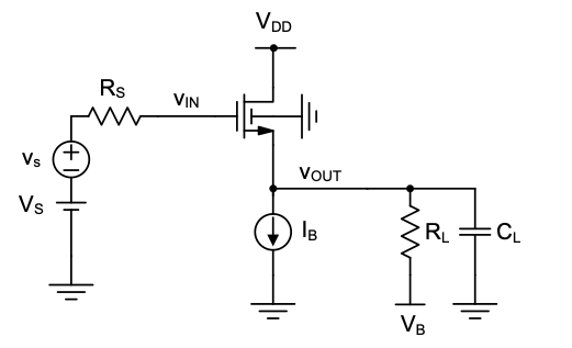
4.4.1 Bias Point Analysis
For a first-pass bias point analysis, consider the circuit in Figure 4.18 first with \(R_L\) disconnected, ensuring that the MOSFET drain current \(I_D = I_B\). Since no current flows into the gate of the MOSFET, we have \(V_{IN} = V_S\). The output voltage quiescent point in this circuit can thus be calculated as already analyzed in the context of the CG stage, using Equation 4.12 with \(V_{IN}\) and \(V_{OUT}\) substituted for \(V_B\) and \(V_S\), respectively.
\[ V_{OUT} = V_{IN} - V_{Tn}(V_{OUT}) - \sqrt{\frac{I_B}{\frac{1}{2} \mu_n C_{ox} \frac{W}{L}}} \tag{4.30}\]
If \(V_B\) at the bottom of \(R_L\) is chosen equal to \(V_{OUT}\) as given in Equation 4.30, no current will flow in this resistor when reconnected and \(I_D = I_B\) is maintained. In cases where this condition is not met, the OSFET’s drain current differs from \(I_B\), but can be computed using iterative calculations. For simplicity in our discussion, we will assume that \(V_B\) (or \(V_{IN}\)) is properly adjusted such that \(I_D = I_B\) is guaranteed.
As far as the MOSFET’s operating region is concerned, it is interesting to note that the device will essentially always operate in the saturation region. This is the case since
\[ V_{DS} = V_{DD} - V_{OUT} = V_{DD} - (V_{IN} - V_{GS}) \tag{4.31}\]
and thus
\[ V_{DS} - (V_{GS} - V_{Tn}(V_{OUT})) = V_{DD} - (V_{IN} - V_{Tn}(V_{OUT})) \tag{4.32}\]
is greater than zero as long as \(V_{IN} < V_{DD} + V_{Tn}(V_{OUT})\), which is almost always the case in a practical realization.
4.4.2 Low-Frequency Analysis
To analyze the circuit’s transfer characteristics at low frequencies, we draw its small-signal model (without any capacitances) as shown in Figure 4.19(a). While this circuit can be analyzed directly by writing nodal equations, it is worth considering a few basic equivalent transformations. First, note that we can split the source controlled by \(v_{gs}\) into two components, \(g_m v_g\) and \(-g_m v_s\), where \(v_g = v_{in}\) and \(v_s = v_{out}\) [see Figure 4.19]. Similarly, the backgate generator is split into \(g_{mb} v_b\) and \(-g_{mb} v_s\), where \(v_b = 0\) (which means that this source can be discarded) and \(v_s = v_{out}\).
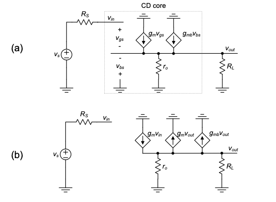
Finally, recognizing that the two sources controlled by \(v_{out}\) are simply resistors of value \(1/g_m\) and \(1/g_{mb}\), we arrive at the final circuit in Figure 4.20.
From this simplified representation, we can immediately see
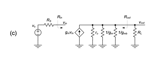
\[ R_{in} \to \infty \tag{4.33}\]
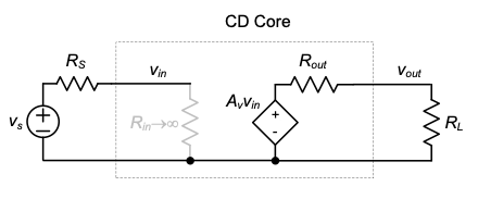
\[ R_{out} = r_o \parallel \frac{1}{g_m} \parallel \frac{1}{g_{mb}} \equiv \frac{1}{g_m + g_{mb}} = \frac{1}{g'_m} \tag{4.34}\]
Consequently, the CD circuit core most closely resembles the properties of a voltage amplifier (high \(R_{in}\), low \(R_{out}\)) and is thus most appropriately modeled using the two-port representation shown in Figure Figure 4.21. The final parameter needed for this model is the open-circuit voltage gain \(A_v\). To find \(A_v\), we apply an ideal test voltage to the circuit of Figure 4.20(c) (i.e., a voltage source with \(R_S = 0\)) and measure the voltage at the open-circuited output port (\(R_L\) disconnected). Neglecting \(r_o\) in this analysis, the reader can prove that
\[ A_v = \frac{g_m}{g_m + g_{mb}} = \frac{1}{1 + \frac{g_{mb}}{g_m}} < 1 \tag{4.35}\]
With \(g_{mb}/g_m\) values on the order of 20% (see Example 4-2), the open-circuit voltage gain of the analyzed n-channel CD stage is on the order of 0.8.
\(A_v\) can approach unity when the source is tied to the bulk of the MOSFET. In this case, \(v_{bs} = 0\), and the \(1/g_{mb}\) resistor in Figure 4.20 is eliminated. Note that for the technology considered in this module, this option is available only for the p-channel version of the circuit. Accordingly, Figure 4.22 summarizes the three different CD configurations that are possible in the assumed technology. In practice, the designer will decide case by case if a source-bulk connection (for the p-channel circuit) is advantageous in the intended application. A disadvantage of the configuration in Figure 4.22(c) is that the bulk-to-substrate (\(C_{bsub}\)) capacitance contributes to the capacitive load of the stage (see Section 4-2 and also Figure 4.26).
Since the CD stage achieves a positive voltage gain near unity, this circuit is often called source follower. The output (the source of the transistor) carries a signal that closely follows the applied input voltage.
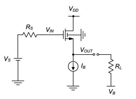
Example 4-5: Low-Frequency Analysis of a CD Amplifier
Consider the CD stage shown in Figure Ex4-5 with the following parameters:
\(V_{DD} = 5 \ \text{V}\), \(V_S = 2.5 \ \text{V}\), \(I_B = 400 \ \mu\text{A}\), \(R_S = 100 \ \text{k}\Omega\) and \(R_L = 5 \ \text{k}\Omega\).
For the MOSFET, assume \(W = 100 \ \mu\text{m}\), \(L = 1 \ \mu\text{m}\), and the standard technology parameters given in Table 4-1. Assume that \(V_B\) is adjusted such that no DC bias current flows in \(R_L\). Calculate \(A_v\), \(R_{out}\), and the overall voltage gain \(v_{out} / v_s\).
SOLUTION
Since the transistor is sized and biased exactly as in the CG stage of Examples 4-3 and Examples 4-4, we know that \(V_{OUT} = 1.273 \ \text{V}\), \(g_m = 2 \ \text{mS}\), and \(g_{mb} = 0.417 \ \text{mS}\).
The resulting open-circuit voltage gain is
\[ A_v = \frac{g_m}{g_m + g_{mb}} = 0.828 \]
and
\[ R_{out} = \frac{1}{g_m + g_{mb}} = 413.8 \ \Omega \]
The overall voltage gain can be computed using Figure 4.21:
\[ A_v' = \frac{v_{out}}{v_s} = A_v \frac{R_L}{R_{out} + R_L} = 0.764 \]
Based on this result, the reader may wonder why the analyzed circuit is useful, as it provides no voltage gain. The benefit of using the stage becomes apparent by comparing to the case where the stage is omitted and \(R_L\) is directly driven by the source. In this case, the voltage gain from \(v_s\) to \(v_{out}\) is given by the resistive divider between \(R_S\) and \(R_L\):
\[ \frac{v_{out}}{v_s} = \frac{R_L}{R_S + R_L} = \frac{5 \ \text{k}\Omega}{100 \ \text{k}\Omega + 5 \ \text{k}\Omega} = 0.048 \]
As we see from this calculation, even though the CD stage does not have voltage gain, it allows us to interface a relatively small load resistance to a source with high source resistance.
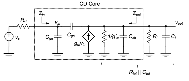
4.4.3 High-Frequency Analysis
To predict the high-frequency behavior of the CD stage, we consider the circuit shown in Figure 4.24. This circuit was constructed using the model of Figure 4.20(c), with all relevant MOSFET capacitances included. Note that \(C_{db}\) is not part of this model, since this capacitance is connected between \(V_{DD}\) and GND (bulk node) and does not influence the signal path. For notational convenience, we define \(C_{tot} = C_L + C_{sb}\) and \(R_{tot} = R_L \parallel \frac{1}{g_m'}\).
The following analysis is partitioned into several steps. First, we will carry out a full KCL-based derivation of the frequency response from first principles. To simplify, we will then customize the obtained general expressions for a specific and typical range of component values. This will greatly simplify the result and also make it amenable for an intuitive interpretation using the Miller theorem. Finally, for the simplified circuit, we will inspect the input and output impedances to construct a two-port model that is valid up to high frequencies.
We begin by noting that the model of Figure 4.24 resembles the CS circuit analyzed in Section 3-3-3: the input and output network are coupled through a capacitor, they contain an RC network on each side, and use a controlled current source in the output network. The main difference lies in the polarity of the controlled source, which reflects the fact that the CD stage is a non-inverting amplifier, whereas a CS stage is an inverting amplifier (i.e., the low-frequency voltage gain is a negative number). This difference has a profound impact on the Miller amplification of the coupling capacitor between the input and output (see Section 3-3-5). We will analyze this in more detail below, after interpreting the general KCL-based result.
Based on the general similarity with the circuit analyzed in Section 3-3-3, we expect that the full transfer function of the CD stage resembles the 2-pole, 1-zero response expressed in Equation 3.38. Indeed, the reader can prove (see Problem 4.9) that carrying out a full KCL-based analysis of the circuit in Figure 4.24 yields
\[ \frac{v_{out}}{v_s} = A_v' \frac{\left(1 + s \frac{C_{gs}}{g_m}\right)}{1 + b_1 s + b_2 s^2} \tag{4.36}\]
where
\[ b_1 = R_s C_{gs} (1 - A_v') + R_s C_{gd} + R_{tot} C_{gs} + R_{tot} C_{tot} \tag{4.37}\]
\[ b_2 = R_s R_{tot} ( C_{gs} C_{gd} + C_{gs} C_{tot} + C_{gd} C_{tot} ) \tag{4.38}\]
and
\[ A_v' = \frac{g_m}{g_m' + \frac{1}{R_L}} \tag{4.39}\]
is the overall low-frequency voltage gain from \(v_s\) to \(v_{out}\).
Once again, while this result is algebraically complex, it is possible to draw a few basic conclusions. First note that the zero in the transfer function occurs at approximately \(\omega_T\), the MOSFET’s cutoff frequency. Hence, the zero will only rarely be relevant for the behavior of the circuit within typical frequencies of interest. Second, if we assume that a dominant pole condition exists, the bandwidth of the circuit will be approximately equal to \(1 / b_1\) (see Section 3-3-4). Note also that the derived \(b_1\) term can alternatively be found using the method of open-circuit time constants (see Section 3-4 and Problem 4-5).
Inspecting Equation 4.37 further, we can consider several approximations. First note that \(R_{tot}\) is a very small resistance \(< 1 / g_m\). Consequently, the time constants \(R_{tot} C_{gs}\) and \(R_{tot} C_{sb}\) (contained in \(R_{tot} C_{tot}\)) are typically not dominant, and we can approximate
\[ b_1 \cong R_s C_{gs} (1 - A_v') + R_s C_{gd} + R_{tot} C_L \tag{4.40}\]
To simplify further, we need to make assumptions about the relative values of \(R_s\) and \(C_L\). This will lead to a result that is no longer general, but useful to capture an important subset of applications for the CD stage. Specifically, consider the circuit shown in Figure 1.5, where the output resistance of a CS stage defines \(R_s\) for the subsequent CD stage. In such an scenario, \(R_s\) will be relatively large and certainly much larger than \(R_{tot}\). Assuming this use case, we can argue that the time constants associated with \(R_s\) will dominate unless a very large load capacitance (greater than \(C_{gs}\)) is connected to the output of the CD stage. Excluding the latter scenario, we arrive at the final approximation \[ b_1 \cong R_s C_{gs}(1 - A_v') + R_s C_{gd} \tag{4.41}\]
With this approximation, the circuit’s bandwidth is \[ \omega_{3\text{dB}} \cong \frac{1}{b_1} \cong \frac{1}{R_s C_{gs}(1 - A_v') + R_s C_{gd}} \tag{4.42}\]
While this result does not hold in general, it applies to an interesting subset of applications, and it also can be interpreted and understood intuitively. Specifically, note that \(C_{gs}\) is modified by a Miller effect multiplier as already seen in Equation 3.51. We can explain the Miller effect multiplier intuitively using Figure 4.25. First note that under the assumption that \(C_L\) is small, the voltage gain from \(v_{in}\) to \(v_{out}\) is constant up to very high frequencies. Hence, this gain can be approximated by its low-frequency value \(A_v'\) (we call this “Miller approximation,” as explained in Section 3-3-5). According to Equation 3.51, the equivalent shunt input capacitance due to \(C_{gs}\) is therefore simply given by \(C_{gs}(1 - A_v')\). Since \(A_v'\) is positive, the portion of \(C_{gs}\) that is seen from the input is reduced by the Miller effect. Circuit designers sometimes referred to as bootstrapping, this effect represents the effective reduction of \(C_{gs}\) in the CD stage, which strongly contrasts with the undesired multiplication of \(C_{gd}\) in a CS stage [see Equation 3.56]. Because of this difference, the bandwidth of a CD stage is often significantly larger than that of a CS stage.
Example 4-6: Bandwidth estimate of a CD Amplifier
Estimate the bandwidth of the CD stage in Figure 4.23 assuming the following parameters: \(R_s = 5\ \text{k}\Omega\), \(R_L = 5\ \text{k}\Omega\), \(g_m = 2\ \text{mS}\), \(g_{mb} = 0.417\ \text{mS}\) (from Example 4-5) and \(C_L = 0\), \(C_{gs} = 203\ \text{fF}\), \(C_{gd} = 50\ \text{fF}\), and \(C_{sb} = 54.3\ \text{fF}\) (from Example 4-4). First perform an estimate on the exact \(b_1\) term given in Equation 4.37, then repeat with the approximate value of Equation 4.41 and compute the discrepancy in percent.
SOLUTION
From Example 4-4, we know that \(A_v'=0.764\). \(R_{tot}\) is the parallel combination of \(1/g_m\), \(1/g_{mb}\), and \(R_L\), which amounts to \(382\ \Omega\). Using Equation 4.37, we can determine the exact value of \(b_1\) as
\[ b_1=R_sC_{gs}(1-A_v')+R_sC_{gd}+R_{tot}C_{gs}+R_{tot}C_{sb} \] \[ =240\ \text{ps}+250\ \text{ps}+78\ \text{ps}+21\ \text{ps}=589\ \text{ps} \]
The corresponding bandwidth estimate is
\(f_{3dB} ≅ \frac{1}{2\pi} \cdot \frac{1}{b_1} = \frac{1}{2\pi} \cdot \frac{1}{589\text{ ps}} = 271 \text{ MHz}\)
According to the approximation of Equation 4.41, we have
\[ b_1 ≅ R_s C_{gs}(1 - A'_v) + R_s C_{gd} = 240\text{ ps} + 250\text{ ps} = 490\text{ ps} \]
Now the corresponding bandwidth estimate is
\[ f_{3dB} ≅ \frac{1}{2\pi} \cdot \frac{1}{b_1} = \frac{1}{2\pi} \cdot \frac{1}{490\text{ ps}} = 325 \text{ MHz} \]
The percent difference between the two estimates is
\[ \frac{325 - 271}{271} = 19.9\% \]
From this result, we see that the simple expression of Equation 4.41 yields a reasonable first-order estimate of the circuit’s bandwidth. The time constants associated with \(R_{tot}\) do not play a significant role in setting the circuit’s bandwidth.
As a final step in our analysis, we now consider the input and output impedances of the CD stage (\(Z_{in}\) and \(Z_{out}\) in Figure 4.24). For \(Z_{in}\), it is clear from the above treatment that
\[ Z_{in} ≅ \frac{1}{s[C_{gs}(1 - A'_v) + C_{gd}]} \tag{4.43}\]
for the given assumptions. An interesting situation arises when a p-channel CD stage with source-bulk tie and purely capacitive load is considered (see Figure 4.24). Since \(A'_v \equiv 1\) in this circuit, the input capacitance is well approximated by \(C_{gd}\) alone, with no significant contribution from \(C_{gs}\). This follows mathematically from Equation 4.43, but, more importantly, makes intuitive sense. When \(A'_v \equiv 1\), the input and output nodes precisely follow the same AC voltage. This means that no AC current can flow through \(C_{gs}\), and hence this capacitance becomes irrelevant.
In order to find \(Z_{out}\), further analysis is needed, and we therefore onsider the setup shown in Figure 4.27. First consider a special situation where \(R_S = 0\). In this case, \(v_{in} = 0\) and the controlled current source is inactive. Thus, we see by inspection
\[ Z_{out} = \frac{1}{g'_m} \, \| \, \frac{1}{s(C_{gs} + C_{sb})} = \frac{1}{g'_m + s(C_{gs} + C_{sb})} \]
\[ = \frac{1}{g'_m} \cdot \frac{1}{1 + s \left( \frac{C_{gs} + C_{sb}}{g'_m} \right)} \equiv \frac{1}{g'_m} \tag{4.44}\]
Here, the final approximation is justified based on the fact that the pole in the preceding expression lies near \(\omega_T\) and is therefore negligible in many cases. Consequently, for the special case of \(R_S = 0\), the output impedance of a CD stage is purely resistive up to very high frequencies and closely approximated by \(1 / g'_m\).
For the case of finite \(R_S\), we write KCL at the two nodes of the circuit and solve for \(Z_{out} = v / i_t\). Approximating \(g'_m \equiv 1 / g_m\) and neglecting \(C_{sb}\) (as justified above) for algebraic simplicity, this yields
\[ Z_{out} \equiv \frac{1}{g_m} \cdot \frac{1 + s(C_{gs} + C_{gd})R_S} {1 + s\left(\frac{C_{gs}}{g_m} + R_S C_{gd}\right) + s^2\left(\frac{R_S C_{gs} C_{gd}}{g_m}\right)} \]
\[ = \frac{1}{g'_m} \cdot \frac{\left( 1 - \frac{s}{z} \right)} {\left( 1 - \frac{s}{p_1} \right) \left( 1 - \frac{s}{p_2} \right)} \tag{4.45}\]
Again, this result is algebraically complex, but can be used to gain some insight into the basic behavior. First, we note that the zero in this expression occurs at a frequency below the approximate bandwidth of the circuit see 4.42. If a dominant pole condition exists, we see that the dominant pole will occur approximately at \(1 / (R_S C_{gd})\) (neglecting \(C_{gs} / g_m = 1 / \omega_T\)). That is, the first pole occurs after the zero in the overall impedance function. This situation is sketched out in Figure 4.28. With the zero occurring first, there is a region in which \(|Z_{out}|\) increases with frequency. This behavior is characteristic of an inductor (the reactance of an inductor is given by \(X = \omega L\)). Consequently, the output impedance
Equation 4.45 can be accurately represented by an equivalent RLC network, see Reference 2 and Problem 4.16. In some practical scenarios, the inductive nature of the output impedance can be problematic due to possible signal oscillations (“ringing”) in response to step-like signals. However, when properly tuned, the inductive component can be used to extend the bandwidth in certain situations. These interesting design topics are unfortunately beyond the scope of the introductory treatment of this module.
In summary, and for the purpose of the multi-stage circuit analysis in Chapter 6, an appropriate (but approximate) two-port model that includes the most relevant impedances is shown in Figure 4.29. This model is reasonably accurate up to frequencies close to the bandwidth of the stage when driven with a relatively large source resistance \(R_S > 1/g_m\). Inductive effects are omitted for simplicity. When confronted with applications that necessitate a different set of approximations, the reader is encouraged to revisit the accurate transfer function result of Equation 4.36 and recustomize it as needed for the specific use case.
4.5 Application Examples of Common-Gate and Common-Drain Stages
In this section we will discuss a few common applications of the CG and CD stages. The discussion is mostly qualitative and is meant to help solidify the qualitative understanding of the basic properties for all stage configurations discussed so far. Further analytical details for a subset of these applications is covered in Chapter 6.
4.5.1 CS-CG Cascade (Cascode Amplifier)
A commonly used circuit called the cascode amplifier combines a CS and CG stage as shown in Figure 4.30. This configuration comes with several benefits, both in terms of low- and high-frequency behavior. From a low-frequency perspective, a key benefit is that the resistance (\(R_{out}\)) looking into the drain of the CG device (\(M_2\)) is extremely high. This follows directly from Equation 4.22, with \(r_s\) substituted by \(r_{o1}\) (the output resistance of MOSFET \(M_1\)), which leads to
\[ R_{out} \equiv r_{o1} \cdot g'_m m_2 r_{o2} \]
Furthermore, note that \(M_1\) essentially operates as a transconductance stage, since its output is taken as a current that feeds into the CG stage formed by \(M_2\). The short-circuit transconductance of the overall cascode circuit is approximately equal to \(g_{m1}\), since M2 merely acts as a unity gain current buffer.
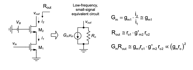
The net effect is that the product \(G_m R_{out}\) of the compound device rmed by \(M_1\) and \(M_2\) is on the order of \((g_m r_o)^2\), the intrinsic voltage gain of a single MOSFET squared. Thus, an important application of the cascode stage turns out to be in operational amplifiers that implement very large voltage gains. An additional application that takes advantage of the large \(R_{out}\) alone is a precision current mirror, discussed in Chapter 5.
Interestingly, the cascode configuration offers high-frequency benefits as well. To see this, consider the two-port model of the cascode stage in Figure 4.31. The capacitance looking into the stage is \(C_{gs1}\) plus the Miller amplified \(C_{gd1}\). However, with \(M_2\) present, the low-frequency voltage gain from the input to the drain node (\(v_x\)) of \(M_1\) (i.e., the Miller gain \(A_{vM}\)) is limited to approximately the ratio of the two device transconductances (provided that \(R_D \ll r_{o2}\)). This means that only a relatively insignificant amount of Miller multiplication occurs; the voltage swing at the circuit output is effectively isolated from the drain node of \(M_1\).
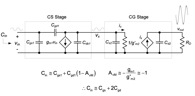
A more subtle but welcome high-frequency benefit comes from reduced feedthrough via \(C_{gd1}\) at very high frequencies. From Equation 3.38, we know that a conventional CS stage comes with a high-frequency zero, defined by the ratio \(g_m' / C_{gd}\). Detailed analysis shows that the pact of this zero on the overall transfer function is largely mitigated with the placement of \(M_2\) between the input and the overall circuit output.
4.5.2 CS-CD Cascade
Another popular two-transistor configuration is the CS-CD cascade shown in Figure 4.32. The main idea here is to employ the CD stage as a voltage buffer to decouple the output resistance of the overall circuit from its voltage gain. Specifically, a relatively large value for \(R_D\) can be used to maximize the voltage gain of the CS stage. Yet, the circuit can drive relatively small load resistors \(R_L\), since the resistance looking into \(M_2\) is small (\(R_{out} \sim 1 / g'_m m_2\)). If \(R_L\) was connected directly to the output of CS stage (\(v_x\)), the voltage gain would reduce significantly (depending on the specific component values).
A disadvantage of using a CD voltage buffer is that the available swing is reduced considerably; this is because the CD device requires a voltage drop of \(V_{Tn} + V_{OV}\) from the gate to the source. This voltage drop reduces the voltage range between \(V_{DD}\) and ground that can be used for the signal.
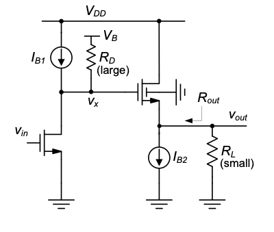
4.5.3 CG Stage as a Load Device
An interesting combination of a CS and CG stage is shown in Figure 4.33. Here, the CG stage essentially emulates the drain resistor \(R_D\) that is shown for example in the stage of Figure 4.32 and used in the CS circuits throughout Chapters 2 and Chapter 3. The small-signal resistance looking into the source of \(M_2\) is approximately \(1 / g'_{m2}\) and therefore the low-frequency voltage gain of the full circuit is approximately equal to \(-g_{m1}/g'_{m2}\). This means that the ain is typically not very large, since there are limits on how small \(g'_{m2}\) can be made while maintaining a reasonable device size.
An advantage of using a MOSFET over a resistor is that the voltage gain is defined by two components of the same type. Circuit designers refer to this concept as ratiometric design. Even if the transconductance of each MOSFET varies substantially (e.g., due to a large temperature change), the voltage gain will remain relatively constant. This concept will be better appreciated once we have discussed sources of parameter variations in Chapter 5.
Similar to the CD buffer discussed in the previous subsection, a disadvantage of this circuit topology is that it does not support a very large output swing. In addition to the voltage drop from the gate to the ource of \(M_2\), note that the output can swing from the quiescent point in the positive direction by at most \(V_{OV2}\) before \(M_2\) enters cutoff.
4.6 Summary
In this chapter, we discussed the common-gate and common-drain stage configurations. As we have seen, the core sections of these circuits operate as a current buffer and voltage buffer, respectively. Figure 4.34 summarizes the corresponding low-frequency model structure in comparison with the common-source stage. Focusing only on the core circuits and cting any auxiliary elements such as drain resistance \(R_D\), Table 4-2 lists the main model parameters. As exemplified in Section 4-5, combining these three configurations with their different characteristics gives the designer the freedom to construct a wide range of application-optimized amplifiers. This idea is studied further in Chapter 6.
As far as the frequency response of the CG and CD stages is concerned, we have seen that several approximations are necessary to capture their essential behavior in simplified, low-complexity expressions. In performing these simplifications and intuitively understanding results that are in their raw form algebraically complex, it pays to master the basic tool set covered in this module so far. Important techniques include the concept of working with unilateral two-port approximations, the dominant pole approximation, the method of open-circuit time constants, and a general feel for the relative magnitudes of MOSFET capacitances, transconductance, and output resistance.
The main finding from the detailed frequency response analysis of the CG and CD stages is that these circuits can operate (under certain conditions) up to very high frequencies, nearing the cutoff frequency (\(\omega_T\)) of the constituent MOSFET.
An important detail in the design of CG and CD stages is the connection of the MOSFET’s bulk. The circuit designer must understand the various options afforded by the process technology and then decide about a suitable configuration that helps maximize performance. As we have shown, it is typically advantageous to connect the bulk to the supply voltage (GND for an n-channel, and \(V_{DD}\) for a p-channel) in a CG stage. In a CD stage, it is sometimes advantageous to opt for a source-bulk tie, especially when a voltage gain as close as possible to unity is required.
| Property | CS | CG | CD |
|---|---|---|---|
| Two-port model | Transconductance or Voltage Amplifier | Current Amplifier | Voltage Amplifier |
| Gain | \(g_m\) or \(A_v = g_m r_o\) | \(A_i ≅ -1\) | \(A_v ≅ 0.7 \dots 1\) |
| \(R_{in}\) | \(\infty\) | \(≅ 1 / g'_m\) | \(\infty\) |
| \(R_{out}\) | \(r_o\) | \(r_o(1 +g'_m r_s)\) | \(≅ 1 / g'_m\) |
4.7 References
R. F. Pierret, Semiconductor Device Fundamentals, Prentice Hall, 1995.
P. R. Gray, P. J. Hurst, S. H. Lewis, and R. G. Meyer, Analysis and Design of Analog Integrated Circuits, 5th Edition, Wiley, 2008.
4.8 Problems
Unless otherwise stated, use the standard model parameters specified in Table 4-1 for the problems given below. Consider only first-order MOSFET behavior and include channel-length modulation (as well as any other second-order effects) only where explicitly stated.
P4.1 In the circuit of Figure 4.35, the MOSFET has a channel length of \(2\ \mu\text{m}\) and the width was chosen such that \(V_{OUT} = 1.5\ \text{V}\) with \(I_B = 200\ \mu\text{A}\). Neglect channel-length modulation.
Draw the complete small-signal model of the circuit and eliminate capacitances that will not affect the circuit operation. Be sure to include the well-to-substrate capacitance.
Calculate the MOSFET’s gate-source (\(C_{gs}\)) and the well-to-substrate (\(C_{bsub}\)) capacitance using the same approach as in Example 4-1. Compute the ratio \(C_{bsub} / C_{gs}\).
P4.2 Repeat Example 4-3 using \(I_B =200\ \text{µA}\) and assuming that the bulk is tied to the source of the MOSFET, i.e., \(V_{SB} = 0\). Recompute \(V_{OUT}\), \(V_S\), as well as \(V_{DS}\) and \(V_{OV} = V_{GS} - V_{Tn}\) of the transistor.
P4.3 The p-channel common-gate amplifier shown in Figure 4.36 has a power dissipation of 1 mW. The MOSFET has a channel length of \(2\ \mu\text{m}\) and the current gain \(i_{out} / i_s = 0.8\). The circuit is biased such that no DC current flows into the resistor connected to the drain.
(a) What is the required \(W\)? For simplicity, neglect the backgate effect in this part of the problem. Also explain why channel-length modulation can be safely ignored.
(b) Re-compute the current gain taking the backgate effect into account (bulk connected to the positive supply). You will need to perform numerical iterations to solve this problem. Based on the results from your first 1–2 iterations, is including the backgate effect worth the effort? Does the current gain increase or decrease relative to part (a)?
P4.4 Repeat Example 4-4 using a channel length of \(3\ \mu\text{m}\) and all other parameters left unchanged. Comment on any changes in the dominant time constants. Note that you will need to recompute the quiescent point voltages of the circuit.
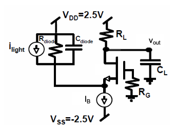
P4.5 The circuit shown in Figure 4.37 is used as a transresistance amplifier for small-signal currents coming from a photodiode, modeled using the equivalent circuit as shown. For simplicity, ignore the backgate effect in all calculations. Parameters:
\(R_{diode} = 50\ \text{k}\Omega\), \(C_{diode} = 70\ \text{fF}\), \(C_L = 150\ \text{fF}\), \(R_L = 1\ \text{k}\Omega\), and \(L = 1\ \mu\text{m}\) for the MOSFET.
Assuming \(I_D = 150\ \mu\text{A}\), calculate the required gate overdrive voltage (\(V_{OV}\)) to achieve a transconductance of \(0.75\ \text{mS}\) and size the width of the transistor accordingly. Determine the proper value needed for \(I_B\) taking \(R_{diode}\) into account. Note that \(R_{diode}\) is a large signal resistance.
Considering only the intrinsic capacitance and ignoring \(r_o\), construct the small-signal model of the circuit.
Calculate the low-frequency transresistance gain \(v_{out} / i_{light}\).
Estimate the circuit’s bandwidth using the method of open-circuit time constants assuming \(R_G = 0\).
Repeat part (d) assuming \(R_G = 500\ \Omega\).
P4.6 Derive the approximate result for the output impedance of a CG stage as given in Equation 4.27. Using the circuit of Figure 4.15, apply a test source at e output and solve for \(Z_{out} = v / i_t\). Simplify the resulting expressions assuming \(\omega \ll \omega_T\) and \(g'_m r_s \gg 1\).
P4.7 Consider the CD circuits shown in Figure 4.38(a) and (b). Ignore channel length modulation.
Suppose that the output voltage swings from \(2\ \text{V}\) to \(4.5\ \text{V}\) in both circuits. Calculate the corresponding voltage swings at the gate nodes for \(R_L = 1\ \text{k}\Omega\) and \(R_L = 1\ \text{M}\Omega\). Determine these values using the transistor’s large signal model. Summarize your results in a table and explain how different values for \(R_L\) and the two bulk connection schemes affect the required input voltages.
Draw a low-frequency small-signal model for the circuit of Figure 4.38(a). ind an analytical expression for the low-frequency small-signal voltage gain \(v_{out} / v_{in}\) as a function of \(R_L\) and the quiescent point voltages \(V_{IN}\) and \(V_{OUT}\). Calculate the small-signal gain at \(V_{OUT} = 2\ \text{V}\) and \(V_{OUT} = 4.5\ \text{V}\) using \(R_L = 1\ \text{k}\Omega\).
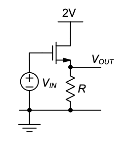
P4.8 In the circuit of Figure 4.39 ignore backgate effect and channel length modulation. Parameters: \(R = 1\ \text{k}\Omega\), \(W/L = 40\).
Calculate the input voltage and corresponding output voltage at which the device enters the triode region.
Sketch \(V_{OUT}\) versus \(V_{IN}\) (\(0 \dots 5\ \text{V}\)). Calculate and annotate pertinent asymptotes and breakpoints, including the voltages calculated in part (a).
P4.9 Derive Equation 4.36 through Equation 4.39 using a KCL-based analysis of the circuit in Figure 4.24.
P4.10 Derive Equation 4.37 by performing an open-circuit time constant analysis for the circuit of Figure 4.24.
P4.11 Consider the p-channel CD circuit of Figure 4.26. Assuming \(C_{gs} = 200\ \text{fF}\) and \(g_m r_o = 50\), what is the contribution of \(C_{gs}\) to the overall input capacitance of the circuit (in fF)?
P4.12 In the circuit of Figure 4.40, the input quiescent point voltage is adjusted such that \(V_{OUT} = 1\ \text{V}\). The MOSFET is sized such that \(V_{OV} = 400\ \text{mV}\) and \(f_T = 1\ \text{GHz}\). In your analysis, neglect backgate effect, finite output resistance, and all extrinsic device capacitances.
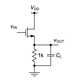
Calculate the circuit’s low-frequency small-signal voltage gain \(v_{out} / v_{in}\).
After playing in the lab for many hours, your friend found that for a certain value of \(C_L\), the circuit achieves a perfectly “flat” frequency response and essentially “infinite” small-signal bandwidth. Calculate the value of \(C_L\) that causes this behavior in \(v_{out}(s)/v_{in}(s)\). Assume that the input of the circuit is driven by an ideal voltage source (\(R_S = 0\)).
Suppose we let \(C_L = 0\). Under this condition, what is the small-signal voltage gain when the input frequency approaches “infinity”? Sketch a Bode plot of the circuit transfer function to justify your answer.
P4.13 In Example 4-6, we estimated the bandwidth of a CD circuit using the term \(b_1\) in the circuit’s transfer function. Given the parameter values used in Example 4-6, plot the magnitude of the exact transfer function given by Eq. (4.36) (using any computer program that is available to you).Find the 3dB bandwidth using a numerical solver. Compare the obtained value with the numbers found in Example 4-6.
P4.14 In Figure 4.25, we used a qualitative reasoning to explain the Miller multiplication term of \(C_{gs}\) in a CD stage. Specifically, we argued that the Miller gain for this capacitance will be constant up to very high frequencies. Following the same approach that was taken to derive Equation 3.54 for the CS stage, derive an exact expression for the Miller gain across \(C_{gs}\) with relevant poles and zeros included. Show that these poles and zeros can be disregarded as long as \(C_L\) is small.
P4.15 Derive Equation 4.45 using a KCL-based analysis. As shown in the circuit of Figure 4.27, apply a test source at the output and solve for \(Z_{out} = v / i_t\). Approximate \(g_m \equiv g'_m\) and neglect \(C_{sb}\).
P4.16 Consider the CD circuit shown in Figure 4.41(a). Neglect finite output resistance and all extrinsic device capacitances, as well as the bulk-to-substrate capacitance.
Draw the small-signal model of the circuit and find a symbolic expression for the output impedance \(Z_{out}(s)\).
Show that for \(R_S > 1 / g_m\), the output impedance can be modeled as an \(RL\) circuit as shown in Figure 4.41(b). Express \(L\), \(R_1\), and \(R_2\) in terms of \(R_S\), \(g_m\), and \(C_{gs}\).
Calculate numerical values for \(L\), \(R_1\), and \(R_2\) assuming the following arameters: \(I_B = 1\ \text{mA}\), \(R_S = 1\ \text{M}\Omega\), \(W = 20\ \mu\text{m}\), and \(L = 1\ \mu\text{m}\). Verify that \(R_S > 1 / g_m\).