2 Transfer Characteristic of the Common-Source Voltage Amplifier
- Review the MOSFET device structure and basic operation as described by the square-law model.
- Introduce large- and small-signal analysis techniques using the common-source voltage amplifier as a motivating example.
- Derive a small-signal model for the MOSFET device, consisting of a transconductance and output resistance element.
- Provide a feel for potential inaccuracies and range limitations of simple modeling expressions.
2.1 First-Order MOSFET Model
The device-level derivations of this section assume familiarity with basic solid-state physics and electrostatics. For a ground-up treatment from first principles, the reader is referred to introductory solid-state device material (see Reference 1).
2.1.1 Derivation of I-V Characteristics
The basic structure of an enhancement mode n-channel MOSFET is shown in Figure 2.1(a). It consists of a lightly doped p-substrate (bulk), two heavily doped n-type regions (source and drain) and a conductive gate electrode that is isolated from the substrate using a thin silicon dioxide layer of thickness \(t_{ox}\). Other important geometry parameters of this device include the channel length \(L\) (distance between the source and drain) and the channel width \(W\).
As we shall see, the name “n-channel” stems from the fact that this device conducts current by forming an n-type layer underneath the gate. A p-channel device can be constructed similarly using an n-type bulk and p-type source/drain regions. The differentiating details between n- and p-channel devices are summarized in Section 2-1-2. For the time being, we will use the n-channel device to discuss the basic principles.
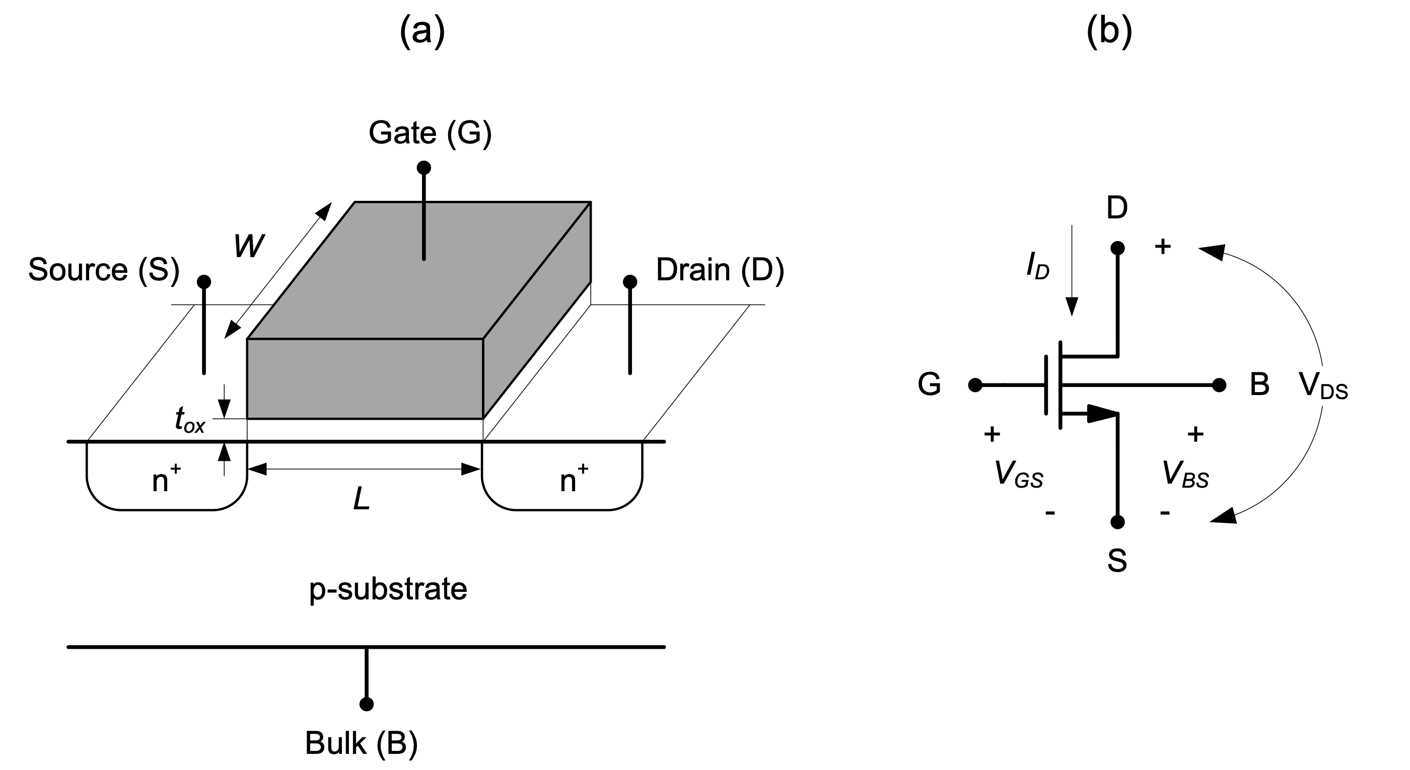
In order to study the electrical behavior of a MOSFET, it is useful to define a schematic symbol and conventions for electrical variables as shown in Figure 2.1(b) . The variables \(V_{GS}\), \(V_{DS}\), and \(V_{BS}\) describe the voltages between the respective terminals using the commonly used ordered subscript convention \(V_{XY}\) = \(V_{X}\) – \(V_{Y}\). The current flowing into the drain node is labeled \(I_{D}\).
It is important to note that the MOSFET device considered here is perfectly symmetric; i.e., the drain and source terminal labels can be interchanged. It is a common convention to assign the source to the lower potential of these two terminals, since this terminal is the source of electrons that enable the flow of current. We will see later that this convention, together with the arrow that marks the source (and the direction of current flow), provides useful intuition when reading a larger circuit schematic.
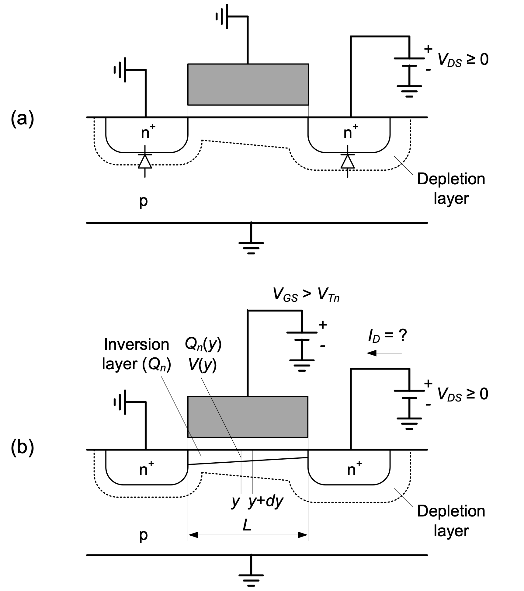
We now begin our analysis of the MOSFET device by considering the condition shown in Figure 2.2(a), where the bulk and source are connected to a reference potential (GND), \(V_{GS}\) = 0 \(V\) and \(V_{DS}\) = 0 \(V\). Under this condition, the drain and source terminals are isolated by two reverse-biased pn-junctions and their depletion regions, which prevent any significant flow of current. Applying a positive voltage at the drain (\(V_{DS}\) > 0 \(V\)) increases the reverse-bias at the drain-bulk junction and will only increase the width of the depletion region at the drain, while \(I_{D}\) = 0 is still maintained (to first-order).
Consider now \(V_{GS}\) = 0 as shown in Figure 2.2(b). This positive voltage at the gate attracts electrons from the source. With increasing \(V_{GS}\), a larger amount of electrons is supplied by the source, and ultimately, a so-called inversion layer forms underneath the gate. The voltage \(V_{GS}\) at which a significant number of mobile electrons underneath the gate become available is called the threshold voltage of the transistor, or \(V_{t}\). In order to differentiate the threshold voltages and other device parameters of n-and p-channel devices, we will utilize the subscripts n and p throughout this module. E.g., we denote the threshold voltage for n-channels and p-channels as \(V_{Tn}\) and \(V_{Tp}\)., respectively.
With the inversion layer under the gate, the drain and source regions are now “connected” through a conductive path and any voltage between these terminals (\(V_{GS}\) > 0) will result in a flow of drain current. How can we calculate this current? In order to answer this question, the following approximations are useful:
1. The current primarily depends on the number of mobile electrons in the channel times their velocity.
2. The number of mobile electrons in the channel is set by the vertical electric field from the gate to the conductive channel (gradual channel approximation).
3. The threshold voltage is constant along the channel; this assumption neglects the so-called body effect.
4. The velocity of the electrons traveling from the source to the drain is proportional to the lateral electric field in the channel.
Figure 2.2(b) establishes relevant variables for further analysis. The auxiliary variable \(y\) ranges from 0 to \(L\) and is used to express electrical quantities as a function of the distance from the source. The inversion layer charge density (per unit area) and voltage at position \(y\) in the channel are denoted as \(Q_{n}(y)\) and \(V_{y}\),respectively. With these conventions in place, we can translate the above-listed assumptions into the following equations:
\[ I_D = - {W} \cdot Q_n \cdot v(y) \tag{2.1}\]
\[ Q_n(y) = -C_{ox} \cdot (V_{GS} - V(y) - V_{Tn}) \tag{2.2}\]
\[ v(y) = -\mu_n \cdot E_y \tag{2.3}\]
In these expressions, \(v\) is the velocity of the carriers, \(C_{ox}\) is the gate capacitance per unit area (between the gate electrode and the conductive channel). The term \(\mu_n\) is called mobility, and it relates the drift velocity of the carriers to the local electric field.
As indicated in Equation 2.2, the mobile charge density at coordinate \(y\) depends on the local potential, since the voltage across the oxide is given by \(V_{GS}\) – \(V(y)\). An inversion layer is present at any location under the gate where this voltage difference is larger than the threshold (\(V_{Tn}\)). Assuming that the inversion layer extends from source to drain as drawn in Figure 2.2(b), we have \(V(L)\) = \(V_{DS}\) and \(Q_{n}\)\((L)\) = –\(C_{ox}\) (\(V_{GS}\) – \(V_{Tn}\) – \(V_{DS}\)). This implies that \(V_{DS}\) cannotexceed \(V_{GS}\) – \(V_{Tn}\) for an inversion layer that extends across the entire channel. For the time being, we will solve for the drain current for this condition and later extend the obtained result for the case of \(V_{DS}\) = \(V_{GS}\) – \(V_{Tn}\).
Now, by combining Equation 2.1 through Equation 2.3 and noting that the electric field is given by \(E(y)=-dV(y)/dy\) , we can write
\[ I_D = \mu_n C_{ox} W \cdot (V_{GS} - V_y - V_{Tn}) \frac{dV_y}{dy} \tag{2.4}\]
This result describes the current density profile along the channel. The terminal current, \(I_{D}\), can be found by separating the variables and integrating along the direction of \(y\)
\[ \int_0^L I_D \, dy = \mu_n C_{ox} W \int_0^{V_{DS}} (V_{GS} - V(y) - V_{Tn}) \, dV \tag{2.5}\]
which yields a closed-form solution for the drain current
\[ \boxed{ I_D = \mu_n C_{ox} \frac{W}{L} \left( V_{GS} - V_{Tn} - \frac{V_{DS}}{2} \right) V_{DS} } \tag{2.6}\]
Note that this expression is valid for \(V_{DS}\) < \(V_{GS}\) – \(V_{Tn}\), as assumed above. In order to extend the obtained result for \(V_{DS}\) = \(V_{GS}\) – \(V_{Tn}\), we continue by inspecting the shape of the inversion layer for various \(V_{DS}\) (see Figure 2.3). For \(V_ {DS}\) = 0 V [case (a)], no current flows and \(V(y)\) = 0 for all \(y\). Provided that \(V_{GS}\) > \(V_{Tn}\), a uniform inversion layer exists underneath the gate. For small \(V_{DS}\) > 0, a current flows in the inversion layer, which causes increasing \(V(y)\) and decreasing inversion layer charge along the channel. As \(V_{DS}\) approaches \(V_{GS}\) - \(V_{Tn}\), \(Q_{n}(L)\) approaches zero with a point of diminishing charge at the drain. This effect is called pinch-off.
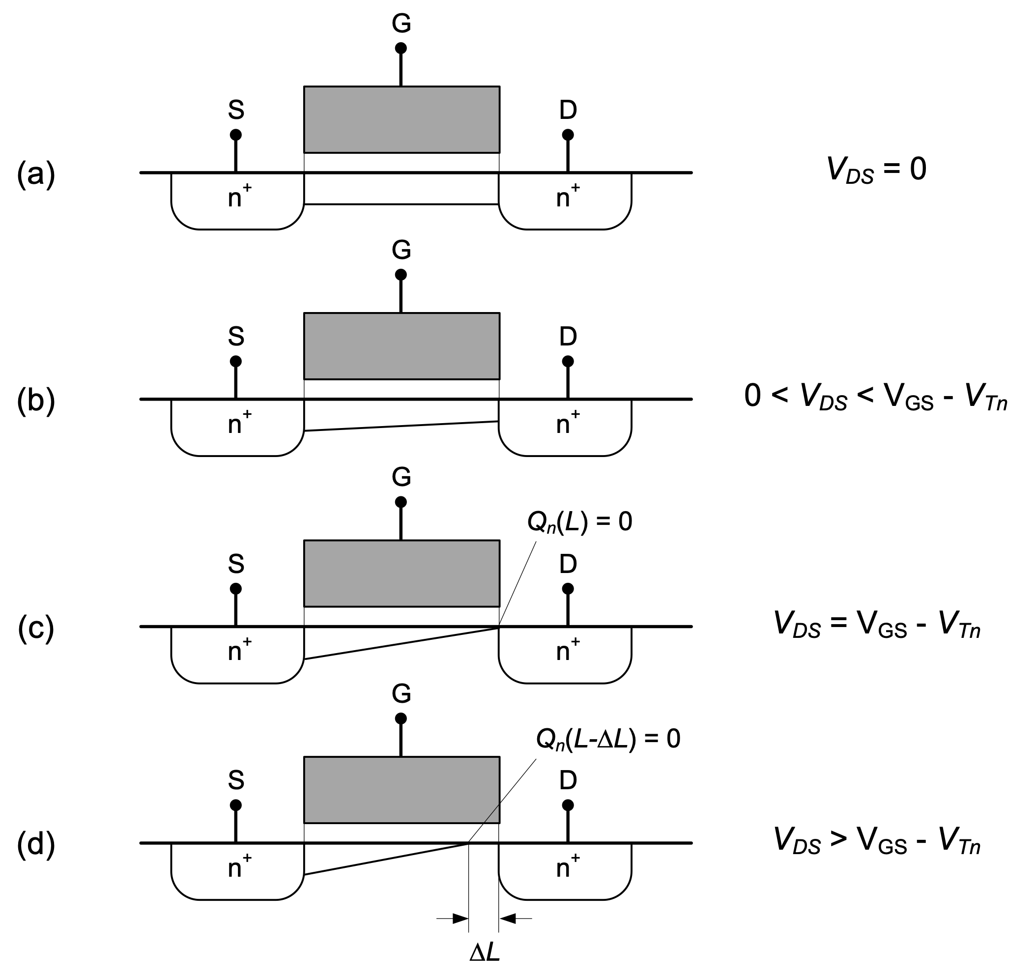
What happens when we increase \(V_{DS}\) beyond the point of pinch-off? Further analysis based on solving the two-dimensional Poisson Equation at the drain predicts that the pinch-off point will move from \(L\) to \(L – ΔL\), where \(ΔL\) is small relative to \(L\). Even though no inversion layer exists in the region from \(L – ΔL\) to \(L\), the device still conducts current. The charges arriving at \(y = L – ΔL\) are being swept to the drain by the electric field present in the depletion region of the surrounding pn junction.
To first-order, and neglecting the small change in channel length \(ΔL\), the current becomes independent of \(V_{DS}\) and is approximately given by the current at the onset of pinch-off, i.e., at \(V_{DS}\) = \(V_{GS}\) – \(V_{Tn}\). Substituting this condition into Equation 2.6, we obtain
\[ \boxed{I_D = \frac{1}{2} \mu_n C_{ox} \frac{W}{L} ({V_{GS}} - V_{Tn})^2} \tag{2.7}\]
for \(V_{DS}\) ≥ \(V_{GS}\) – \(V_{Tn}\).
Equation 2.6 and Equation 2.7 are plotted in Figure 2.4 as a function of \(V_{DS}\) and some fixed \(V_{GS}\) > \(V_{Tn}\). The operating region for \(V_{DS}\) < \(V_{GS}\) – \(V_{Tn}\) is commonly called the triode region. This name stems from the direct dependence of the drain current on the drain-source voltage, which is qualitatively similar to the behavior of vacuum tube “triodes.” The region \(V_{DS}\) ≥ \(V_{GS}\) – \(V_{Tn}\) is called the saturation region due to the saturation in current at large \(V_{DS}\). In this region, the device operates essentially like a current source; the current is (to first-order) independent of the applied \(V_{DS}\) and \(I_{D}\) = \(I_{Dsat}\) = constant. The quantity \(V_{GS}\) – \(V_{Tn}\) is often called gate overdrive.
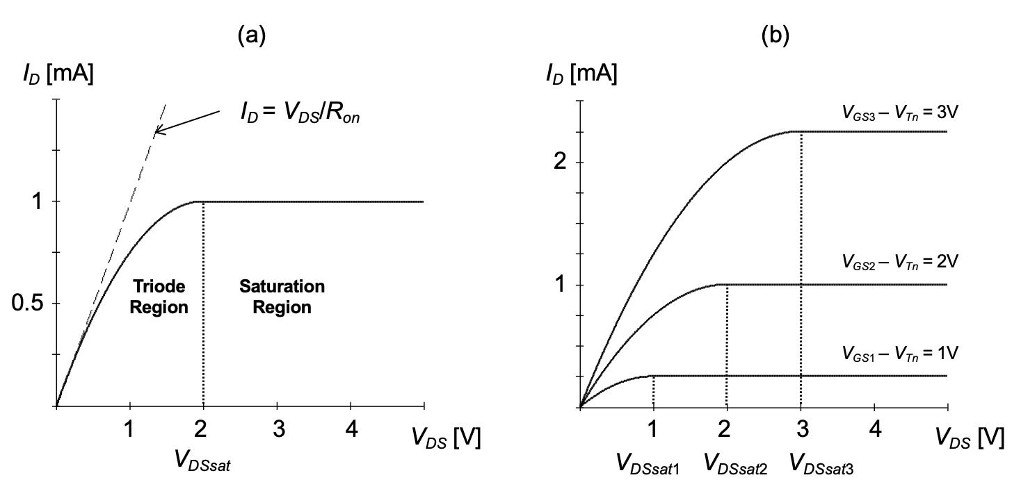
The drain-source voltage at which the drain current saturates is called \(V_{DSat}\). From the above first-order analysis, it is clear that \(V_{DSat}\) = \(V_{GS}\) – \(V_{Tn}\). Nonetheless, it is useful to distinguish between these two quantities, because they may differ significantly when a more elaborate device model is used. \(V_{DSat}\) is generally not exactly equal to \(V_{GS}\) – \(V_{Tn}\) when second-order effects, for example related to small geometries and modern device structures, are considered.
From a circuit perspective, the device’s behavior in the triode region is similar to a resistor: the current increases monotonically with increasing terminal voltage. Even though the dependence of \(I_{D}\) on \(V_{DS}\) is nonlinear (as seen from Equation 2.6), it is sometimes useful to approximate the characteristic using a linear I-V law, shown as a dashed line in Figure 2.4(a). For \(V_{DS}\) \(\ll\) \(V_{GS}\) – \(V_{Tn}\) , we can approximate Equation 2.6 as
\[ I_D \equiv \mu_n C_{ox} \frac{W}{L} (V_{GS} - V_{Tn}) V_{DS} \tag{2.8}\]
Under this approximation, \(I_{D}\) depends linearly on \(V_{DS}\), and we can define the so-called on-resistance of the device as
\[ R_{on} = \frac{V_{DS}}{I_D} \equiv \frac{1}{\mu_n C_{ox} \frac{W}{L} (V_{GS} - V_{Tn})} \tag{2.9}\]
It is interesting to interpret the dependencies in this expression using basic intuition. Increasing the aspect ratio \(W /L\) decreases \(R_{on}\) since the conductive path becomes shorter and/or wider; this is a basic property of any conductor. The on-resistance also decreases with increasing \(C_{ox}\) and \(V_{GS}\) – \(V_{Tn}\); this is because the inversion charge increases with these quantities (\(Q = CV\)). Larger mobility (\(μ_{n}\)) means that the carriers travel faster for the same applied voltages (electric field). This increases the current (charge per unit of time) and therefore also results in smaller \(R_{on}\).
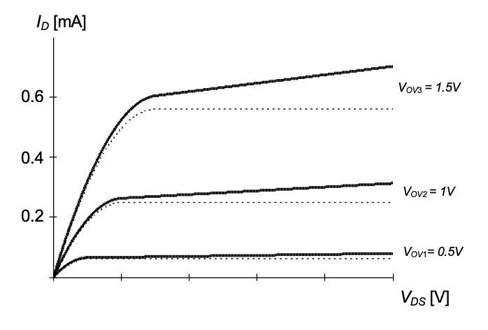
As seen from Equation 2.7, the magnitude of the drain current in saturation depends on the square of the gate overdrive \(V_{GS}\) – \(V_{Tn}\). This is further illustrated in Figure 2.4(b), which shows I-V plots for increasing multiples of \(V_{GS1}\) – \(V_{Tn}\) = 1V. Doubling and tripling the gate overdrive increases the saturation current by factors of four and nine, respectively. Note that \(R_{on}\) is reduced only by factors of two and three in these cases, respectively.
The plot in Figure 2.4(b) is often called the drain characteristic, because the drain-source voltage (as opposed to the gate-source voltage, which is included as a parameter on the curves), is swept along the x-axis. Alternatively, the term output characteristic is sometimes used, primarily because \(V_{DS}\) can often be viewed as the output port voltage of the device; we will see this in the example discussed in Section 2-2.
Another commonly used characterization plot for MOSFETs is the so-called transfer characteristic, which shows the drain current as a function of \(V_{GS}\) for a fixed value of \(V_{DS}\). If \(V_{DS}\) is chosen large enough such that the device operates in the saturation region for all applied \(V_{GS}\), \(I_{D}\) follows from Equation 2.7 and the plot is shaped like a parabola as drawn in Figure 2.5.
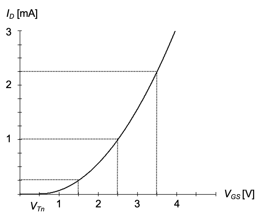
Table 2.1 summarizes the first-order MOSFET I-V relationships that were discussed in this section. This set of equations (and extended versions thereof) is often called the square-law model since one of its primary features is the quadratic dependence of the saturation current on \(V_{GS}\) – \(V_{Tn}\). When working with this device model, it is important to remember that it predicts the behavior of real MOSFETs only with limited accuracy. This is primarily so because we have made several simplifications in the model’s derivation. The most significant shortcom ings that result from these assumptions can be summarized as follows:
In reality, the saturation current has a weak dependence on \(V_{DS}\). This is primarily due to a shortening of the channel length (\(ΔL\)) with increasing \(V_{DS}\) and also due to the drain voltage dependence of the mobile charge in the channel. We will address this issue in Section 2-2.
For transistors built in modern technologies, several second-order effects related to small geometries and large electric fields become significant. This typically results in a saturation current law exponent that is less than two, and \(V_{DSat}\) < \(V_{GS}\) – \(V_{Tn}\). In addition, the drain current does not scale strictly proportional to \(1/L\) and the threshold voltage is not constant, but a function of the drain voltage.
For \(V_{GS}\) < \(V_{Tn}\) the device is not completely off, but carries a small current that exponentially depends on \(V_{GS}\). This operating region is called the sub-threshold region.
For small values of \(V_{GS}\) < \(V_{Tn}\), on the order of a few tens of millivolts, the region underneath the gate is only moderately inverted, and the square law model tends to predict the drain current with poor accuracy.
“ON” \(V_{GS} ≥ V_{Tn}\) |
“OFF” \(V_{GS} < V_{Tn}\) |
|
|---|---|---|
| \(V_{DS} < V_{DSat}\) | \(I_D = \mu_n C_{ox} \frac{W}{L} (V_{GS} - V_{Tn} - \frac{V_{DS}}{2}) V_{DS}\) | \(I_D = 0\) |
| \(V_{DS} \geq V_{DSat}\) | \(I_D = \frac{1}{2} \mu_n C_{ox} \frac{W}{L} (V_{GS} - V_{Tn})^2\) | \(I_D = 0\) |
Despite these shortcomings, the first-order MOSFET model possesses many of the critical features needed to study the fundamentals of analog circuit design. Many of the second-order effects not featured in the basic model can be treated using advanced device physics and often result in a high-complexity model that is unsuitable for hand-calculations and intuition building.
Within the range of circuits treated in this mod ule, we typically begin by applying the first-order model. Then, only when the circuit appears to be sensitive to second-order dependencies not covered by this model, we will look for extensions. A treatment in this fashion has the advantage that the reader can develop a feel for where and when modeling extensions and parameter accuracy are critical.
In general, the tradeoff between modeling accuracy and complexity is a recurring theme at all levels of analog circuit design; the issue is not limited to the introductory material covered in this module. More accurate models can always be generated at the expense of complexity and time. An experienced analog designer will often use the simplest possible model that will predict the behavior of his or her circuit with sufficient (but not perfect) accuracy. This also implies that analog circuit designers must always be on the lookout for model inadequacies. We will encounter and discuss situations where either model expansions or critical insight on modeling accuracy are needed throughout this module.
2.1.2 P-Channel MOSFET
The n-channel MOSFET discussed so far conducts current through an electron inversion layer in a p-type bulk. Similarly, we can construct a p-channel device that operates based on forming an inversion layer of holes in an n-type bulk. The structure of such a MOSFET, which consists of \(p+\) source and drain regions in an n-type bulk, is shown in Figure 2.6. In many process technologies, the n-type bulk region is formed by creating an n-type well (n-well) in the p-type substrate that is used to form n-channels. Such a technology is called an n-well technology. In general, a technology that offers both n- and p-channel devices is called CMOS technology, where CMOS stands for Complementary Metal-Oxide-Semiconductor.
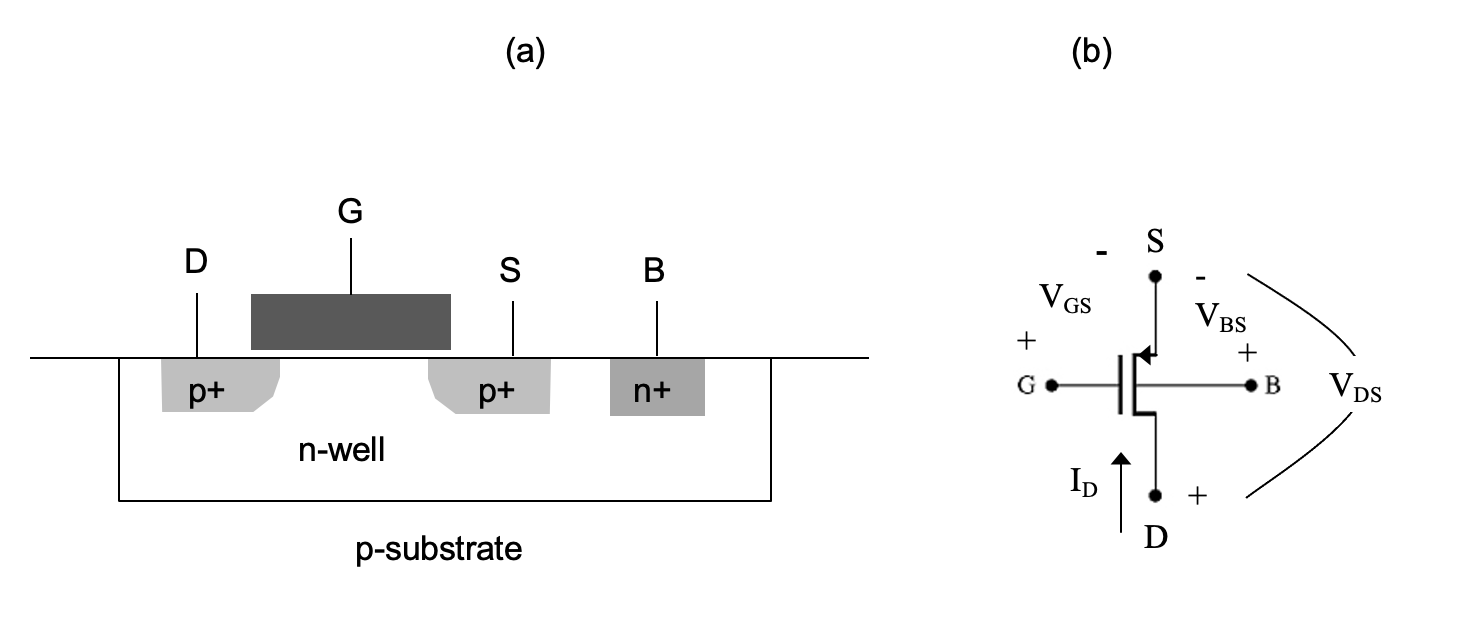
The drain current equations for a p-channel MOSFET can be derived using exactly the same approach as used for the n-channel device since the basic physics are the same. For a p-channel device, the gate must be made negative with respect to the p-type source in order to form an inversion layer of holes; the threshold voltage \(V_{Tp}\) is therefore typically negative. Since holes drift across the channel from the source to the drain in the p-channel MOSFET, the drain voltage must be negative with respect to the source, and the drain current (defined as flowing into the drain terminal) is negative. Therefore, in the on-state of the transistor, \(V_{GS}\) and \(V_{DS}\) are negative quantities, and the source lies at the highest potential among the four terminals. The drain current for a p-channel in saturation, i.e., \(V_{GS}\) < \(V_{DS}\) and \(V_{DS}\) ≤ \(V_{GS}\) – \(V_{Tp}\), is given by
\[ {I_D = -\frac{1}{2} \mu_p C_{ox} \frac{W}{L} ({V_{GS}} - V_{Tp})^2} \tag{2.10}\]
A practical problem for the circuit designer is to keep track of the minus signs and negative quantities in the p-channel equations. A solution to this issue is to “think positive,” and work with the physically intuitive positive quantities \(V_{SG}\) (instead of \(V_{GS}\)), \(V_{SD}\) (instead of \(V_{DS}\)) in all hand calculations. Following this approach, we can rewrite Equation 2.10 as
\[ -{I_D = \frac{1}{2} \mu_p C_{ox} \frac{W}{L} ({V_{GS}} - V_{Tp})^2} \tag{2.11}\]
Note that the right-hand side of this equation yields a positive number. The minus sign included on the left-hand side remains necessary because \(I_D\), as defined in Figure 2.6(b), is a negative quantity.
2.1.3 Standard Technology Parameters
For use throughout this module, it is convenient to define standard MOSFET parameter values as given in Table 2.2. The chosen values are representative of a CMOS technology with a minimum channel length, or feature size of 1 \(\mu\)m. As we learn more about the behavior of MOSFETs in later sections, this list of parameters will grow and we will augment it as needed.
In the context of defining these parameters, it is important to make a clear distinction between technology parameters and design parameters. Technology parameters are typically fixed in the sense that a circuit designer cannot alter their values. For instance, the mobility in a MOSFET depends on how the transistor is made, and the underlying recipe remains unchanged and will be reused for an extended time to manufacture a large variety and quantity of integrated circuits. In most modern CMOS technologies, the width and length of a MOSFET remain as the only parameters that the circuit designer can choose (within appropriate limits) to alter the device’s electrical behavior.
In determining the transistor geometries, the designer will usually work with electrical variables and parameters that describe the circuit and its functionality, for example in terms of currents and voltages. From these electrical descriptions and specifications, the widths and lengths of the transistors are then calculated, and sometimes adjusted via an iterative process. In this task, intermediate electrical parameters, as for instance the gate overdrive of a MOSFET, are also legitimately viewed as parameters that are under the control of the circuit designer.
Example 2-1: P-Channel Drain Current Caculation
A p-channel transistor is operated with the following terminal voltages relative to ground: \(V_{G}\) = 2.5 \(V\), \(V_{S}\) = \(V_{B}\) = 5 \(V\), \(V_{D}\) = 1 \(V\). Calculate the drain current \(I_D\) using the standard technology parameters given in Table 2.2 and assuming \(W/L = 5\).
SOLUTION
From the given terminal voltages, we find \(V_{SG}\) = 5 \(V\)– 2.5 \(V\) = 2.5 \(V\) and \(V_{SD}\) = 5 \(V\) – 1 \(V\) = 4 \(V\). Since \(V_{SG}\) > \(V_{Tp}\), the transistor is on, and since \(V_{SD}\) > \(V_{SG}\) + \(V_{Tp}\) = 2.5 \(V\) – 0.5 \(V\) = 2 \(V\), it operates in saturation. Therefore, using Equation 2.11 we find
\[ -{I_D = \frac{1}{2} \mu_p C_{ox} \frac{W}{L} ({V_{GS}} - V_{Tp})^2} \] \[ -{I_D = \frac{1}{2} \cdot 25\frac{μA}{V^2} \cdot 5 \cdot (2.5 V - 0.5V)^2 = 250μA} \]
\[ -I_D = -250μA \]
| Parameter | n-channel MOSFET | p-channel MOSFET |
|---|---|---|
| Threshold voltage | \(V_{Tn}\) = 0.5V | \(V_{Tp}\) = -0.5V |
| Transconductance parameter | \(μ_nC_{ox}= 50μA/V^2\) | \(μ_pC_{ox}= 25μA/V^2\) |
2.2 Building a Common-Source Voltage Amplifier
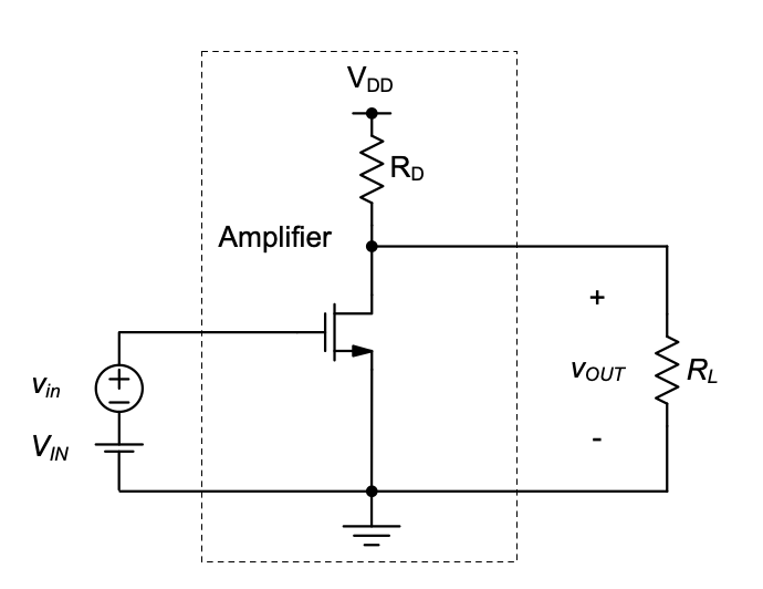
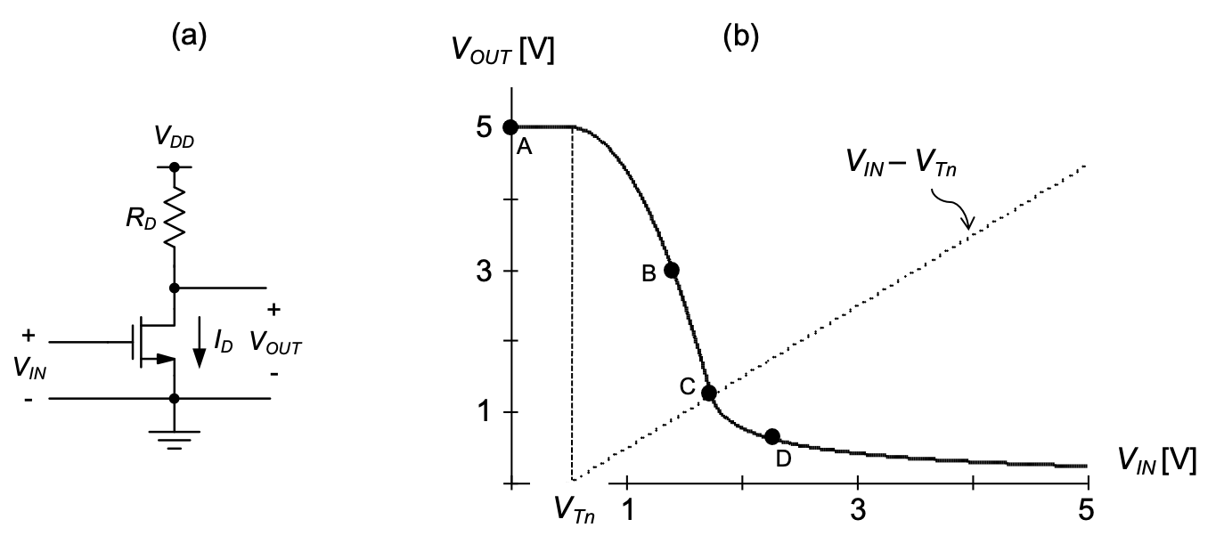
We will now utilize our first-order understanding of MOSFETs to construct a basic voltage amplifier. We begin by noting that the drain current in all regions of operation can be controlled by varying the gate-source voltage. One way to utilize this effect to build a voltage amplifier is to apply the input such that it controls \(V_{GS}\). An output voltage can then be generated by letting the drain current flow through a resistor, as shown in Figure 2.7(a). The top terminal of the resistor is connected to a supply voltage, \(V_{DD}\). In this scheme, a larger \(V_{IN}\) causes the drain current to increase and \(V_{OUT}\) to decrease, since a larger \(V_{IN}\) makes the transistor a “better conductor” (more inversion charge), which forces the voltage at the output port closer to ground. This type of circuit is therefore categorized as an inverting amplifier. Furthermore, this transistor stage is called a common-source amplifier, since the source terminal of the MOSFET is common to the input and output ports of the circuit.
2.2.1 Voltage Transfer Characteristic
In order to derive the voltage transfer characteristic of the circuit (\(V_{OUT}\) as a function of \(V_{IN}\)) we begin by applying Kirchhoff’s laws at the output node. This yields
\[ V_{OUT} = V_{DD} - I_D R_D \tag{2.12}\]
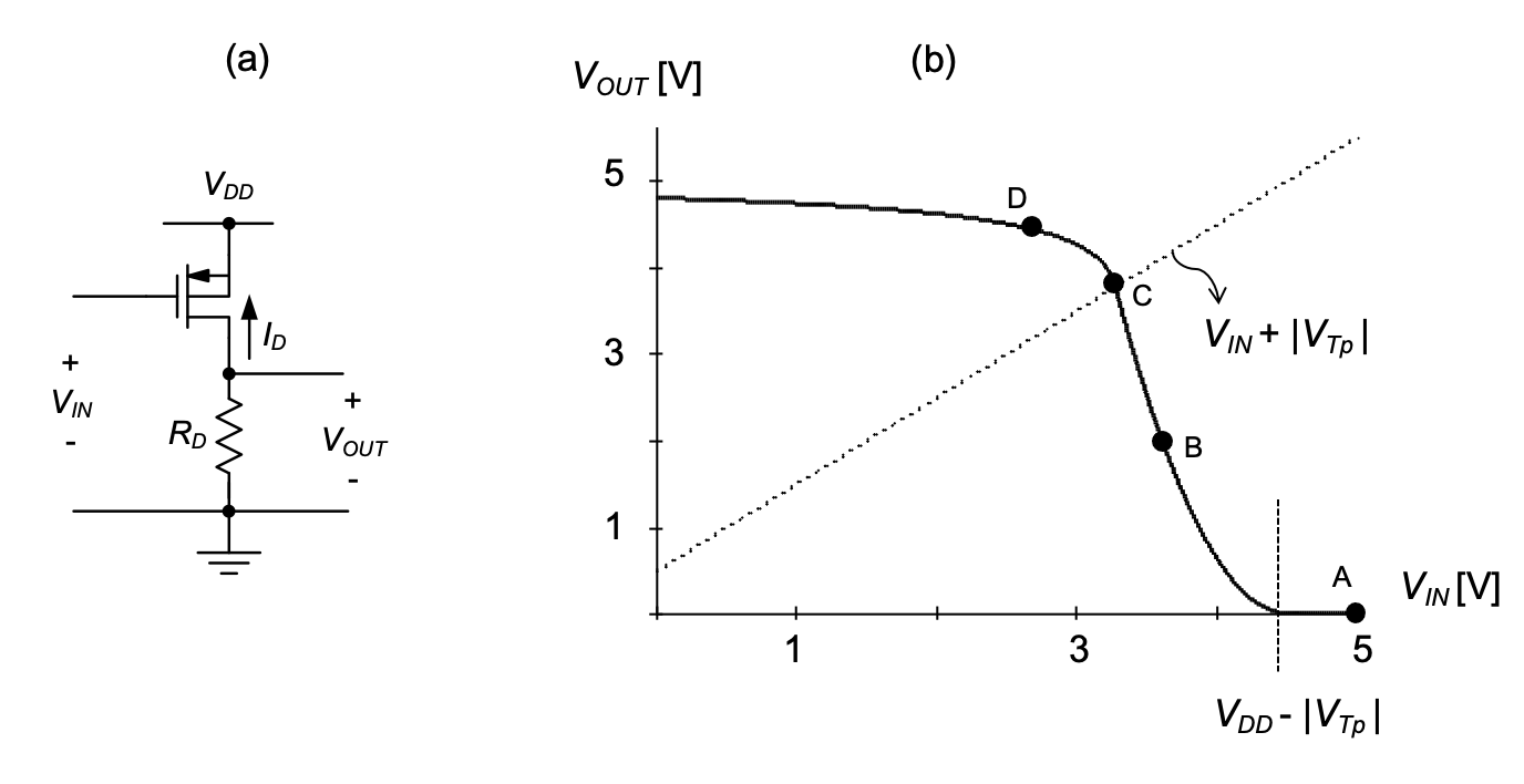
The drain current ID in this expression depends on \(V_{GS}\) and \(V_{DS}\) of the transistor, as described in Table 2.1. Given the structure of the circuit in Figure 2.7(a), we note that \(V_{GS}\) = \(V_{IN}\) and \(V_{DS}\) = \(V_{OUT}\). Using this information, we can construct a piecewise function that relates the input and output voltages of the circuit. For this derivation, imagine that we sweep \(V_{IN}\) from 0 \(V\) to the supply voltage, \(V_{DD}\).
First, we note that for \(V_{IN}\) = \(V_{GS}\) < \(V_{Tn}\), no current flows in the transistor; this implies \(V_{OUT}\) = \(V_{DD}\). This behavior is shown in Figure 2.7(b) as a horizontal line for the input voltage range 0 ≤ \(V_{IN}\) < \(V_{Tn}\), between points A and the vertical line at \(V_{Tn}\). As \(V_{IN}\) increases to values greater than or equal to \(V_{Tn}\), the transistor conducts current, and \(V_{OUT}\) must be less than \(V_{DD}\). In order to calculate how \(V_{OUT}\) changes as a function of \(V_{IN}\), we must first determine the transistor’s region of operation. As we increase \(V_{IN}\) above \(V_{Tn}\), does the MOSFET operate in saturation or in the triode region?
To answer this question, we must determine if \(V_{DS}\) is smaller or larger than \(V_{GS}\) - \(V_{Tn}\). For \(V_{IN}\) just above \(V_{Tn}\), \(V_{GS}\) – \(V_{Tn}\) is smaller than \(V_{DS}\), which is still close to \(V_{DD}\) at the onset of current conduction. Therefore, the device must initially operate in saturation as we transition from the “OFF” state of the transistor into the region where \(I_D\) > 0. Under this condition, the output voltage is given by
\[ V_{OUT}=V_{DD} - R_D \cdot \frac{1}{2} \mu_n C_{ox} \frac{W}{L}(V_{IN}-V_{Tn})^2 \tag{2.13}\]
and the voltage transfer characteristic shows a drop that is quadratic in \(V_{IN}\) as seen in Figure 2.7(b).
As we continue to increase \(V_{IN}\), \(V_{GS}\) - \(V_{Tn}\) also increases while \(V_{OUT}\) continues to decrease. At a sufficiently large \(V_{IN}\), \(V_{DS}\) can approach \(V_{GS}\) - \(V_{Tn}\) and the condition for current saturation may no longer hold; the device then transitions into the triode region. The input voltage at which this transition occurs (point \(C\) in Figure 2.7(b)) can be computed by setting the right-hand side of Equation 2.13 equal to \(V_{IN}\) – \(V_{Tn}\), and solving for \(V_{IN}\). It is interesting to note that graphically, point \(C\) can be found through the intersection of the voltage transfer characteristic with the line \(V_{IN}\) – \(V_{Tn}\). The intersect corresponds to the point where \(V_{OUT}\) = \(V_{DS}\) = \(V_{IN}\) – \(V_{Tn}\) = \(V_{GS}\) - \(V_{Tn}\), i.e., the transition point between saturation and triode for the MOSFET.
For the region where the MOSFET operates in the triode region, we have
\[ V_{OUT} = V_{DD}-R_D \cdot \mu_n C_{ox}\frac{W}{L}(V_{IN}-V_{Tn}-\frac{V_{OUT}}{2})V_{OUT} \tag{2.14}\]
Unfortunately, solving this expression for \(V_{OUT}\) yields an unwieldy square-root expression that is best analyzed graphically. As we can see from the plot in Figure 2.7(b), the most important feature here is that the slope of the voltage transfer characteristic diminishes for large \(V_{IN}\); i.e., the slope of the curve at point \(D\) is smaller than the slope at point \(C\). Qualitatively, this can be explained by viewing the MOSFET as a resistor, whose value continues to decrease with \(V_{IN}\). For very large \(V_{IN}\), the output voltage must asymptotically approach 0 V. This can be shown by approximating the MOSFET by its on-resistance for small \(V_{DS}\) as given by Equation 2.9. The output voltage in the vicinity of point \(D\) can then be expressed by considering the resistive voltage divider formed by \(R_{D}\) and \(R_{on}\).
\[ V_{OUT}≅\frac{V_{DD} \cdot R_{on}}{R_D + R_{on}} = \frac{V_{DD}}{1+R_D\cdot\mu_n C_{ox}\frac{W}{L}(V_{IN}-V_{Tn})} \tag{2.15}\]
This result confirms that for large input voltages, \(V_{OUT}\) will asymptotically approach zero.
Example 2-2: Voltage Transfer Calculations for a Common-Source Amplifier
Consider the circuit of Figure 2.7(a) with the following parameters: \(V_{DD}\) = 5 \(V\), \(R_D\) = 10 \(kΩ\).
Using the standard technology parameters of Table 2.2, calculate the required aspect ratio \(W/L\) such that \(V_{OUT}\) = 2.5 \(V\) for \(V_{IN}\) = 1 \(V\).
Assuming \(W/L\) =10, calculate the input voltage \(V_{IN}\) that yields \(V_{OUT}\) = 2.5 \(V\).
SOLUTION
- As a first step, we can calculate the drain current that results in \(V_{OUT}\) = 2.5 \(V\) using Equation 2.12.
\[ V_{OUT} = V_{DD}-I_D R_D \] \[ 2.5V = 5V - (I_D\cdot 10kΩ ) \] \[ I_D= 250µA \]
Since \(V_{GS}\) – \(V_{Tn}\) = 0.5 V < \(V_{DS}\) = 2.5 V, we know that the device must operate in the saturation region. Therefore,
\[ I_D = \frac{1}{2} \mu_n C_{ox} \frac{W}{L} ({V_{GS}} - V_ {Tn})^2 \] \[ 250µA= \frac{1}{2}\cdot 50\frac{µA}{V^2}\cdot\frac{W}{L} \cdot(1V-0.5V)^2 \]
and solving for the aspect ratio yields \(W/L = 40\). Note that this answer can also be found by direct evaluation of Equation 2.13, without computing \(I_D\) initially.
- since \(V_{IN}\) is unknown in this part of the problem, we cannot immediately determine the operating region of the MOSFET. In such a situation, it is necessary to guess the operating region, and later test whether the guess was correct. Let us begin by assuming that the device operates in saturation. We can then write
\[ I_D = \frac{1}{2} \mu_n C_{ox} \frac{W}{L} ({V_{GS}} - V_{Tn})^2 \] \[ 250µA= \frac{1}{2}\cdot 50\frac{µA}{V^2}\cdot 10 \cdot(V_{GS}-0.5V)^2 \]
The two solutions to this equation are \(V_{GS1}\) = 1.5 \(V\), and \(V_{GS2}\) = –0.5 \(V\). Since we know that the device is off for \(V_{GS}\) < \(V_{Tn}\), it is clear that \(V_{GS2}\) is a non-physical solution that must be discarded. For the obtained \(V_{GS1}\), we must now verify that the device operates in saturation, as initially assumed. It is straightforward to see that this is indeed the case since \(V_{GS1}\) – \(V_{Tn}\) = 1 \(V\)< \(V_{DS}\) = 2.5 \(V\). Therefore, the final answer to this problem is \(V_{IN}\) = 1.5 V.
If we had initially guessed that the device operates in the triode region, we would write
\[ I_D=\mu_n C_{ox}\frac{W}{L}(V_{GS}-V_{Tn}-\frac{V_{DS}}{2})V_{DS} \] \[ 250µA = 50\frac{µA}{V^2}\cdot 10 \cdot (V_{GS} - 0.5V - \frac{2.5V}{2})\cdot 2.5V \]
- The two solution to this equation is \(V_{GS}\) = 1.95 \(V\). Since \(V_{GS}\) – \(V_{Tn}\) = 1.45 \(V\) < \(V_{DS}\) = 2.5, we see that the obtained result contradicts the assumed operation in triode. Therefore, the next logical step would be to evaluate the saturation equation, as already done above.
2.2.2 Load Line Analysis
A generally useful tool for graphical analysis in electronic circuits is the so-called load line analysis. The basis for such an analysis in the context of our circuit is the fact that the current flowing through the transistor (\(I_D\)) is equal to the current flowing through the resistor (which is viewed in this context as the load of the circuit). Therefore, if we draw the I-V characteristics of the MOSFET and \(R_D\) in one diagram, valid output voltages lie at the intersection of the two curves (equal current). This is further illustrated in Figure 2.8. The load line equation in this plot follows from solving Equation 2.12 for \(I_D\) and is given by
\[ I_D= \frac{V_{DD} - V_{OUT}}{R_D} \tag{2.16}\]
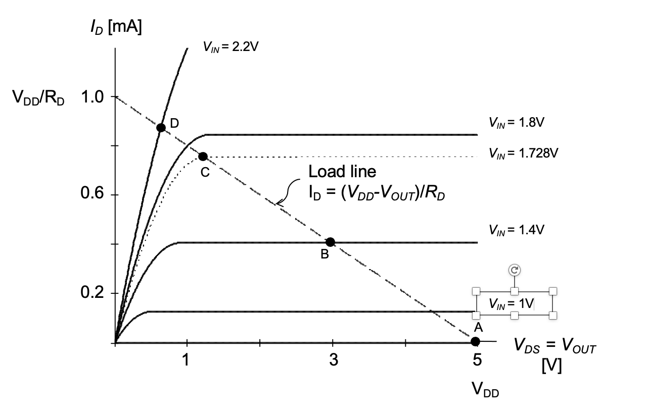
The points A, B, C, and D marked in Figure 2.8 correspond to the points shown with the same annotation in Figure 2.7(b). Since the transistor drain characteristics are overlaid in Figure 2.8, it is easy to identify the operating regions that correspond to each point. For example, we can immediately see that point B lies in saturation, since the intersect occurs in a region of constant drain current.
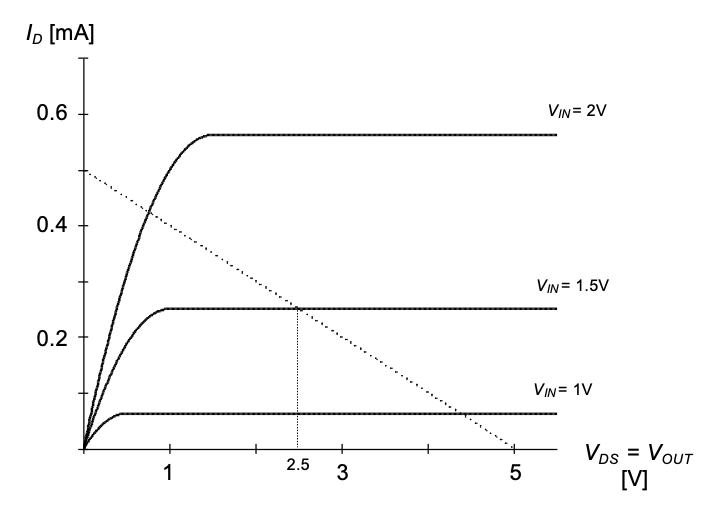
Example 2-3: Output Voltage Calculations for a Common-Source Voltage Amplifier
Construct a load line plot to verify the solution of Example 2-2(b) using \(V_{DD}\) = 5 \(V\), \(R_D\) = 10 kΩ , and W/L =10. Use \(V_{IN}\) = \(V_{GS}\) = 1 \(V\), 1.5 \(V\), and 2 \(V\) for the drain characteristic plot.
SOLUTION
The solution is shown in Figure 2.9. The load line is most easily drawn by connecting the points (0, \(V_{DD}\)/\(R_D\) = 0.5 \(mA\)) and (\(V_{DD}\) = 5 \(V\), 0). The drain characteristics are drawn for the three given \(V_{GS}\) using the expressions of Table 2.1, by sweeping \(V_{DS}\) = \(V_{OUT}\) from 0 \(V\) to 5 \(V\). The intersect of the load line with the drain characteristic for \(V_{IN}\) = 1.5 \(V\) confirms the result already obtained in Example 2-2(b).
2.2.3 Biasing
After deriving the voltage transfer characteristic of our amplifier, we are now in a position to evaluate this circuit from an application standpoint. As we have discussed in Chapter 1, a common objective for a voltage amplifier is to create large output voltage excursions from small changes in the applied input voltage. With this objective in mind, it becomes clear that only a limited range of the transfer characteristic in Figure 2.7(b) is useful for amplification. For example, a change in the input voltage applied around point D in Figure 2.7(b) yields almost no change in the output voltage. In order to amplify small changes in \(V_{IN}\) into large changes in \(V_{OUT}\), the transistor should be operated in the saturation region, i.e., in the vicinity of point B. The general concept of operating a circuit and its constituent transistor(s) around a useful operating point is called biasing.
Biasing generally necessitates the introduction of auxiliary voltages and/or currents that bring the circuit into the desired state. For the circuit considered in this section, proper biasing can be achieved by decomposing the input voltage into a constant component, and a component that represents the incremental voltage change to be amplified; this is illustrated in Figure 2.10(a). The incremental voltage component \(v_{in}\) could represent, for instance, the signal generated by a microphone or a similar transducer. The voltage \(V_{IN}\) is a constant voltage that defines the point on the overall transfer characteristic around which the incremental \(v_{in}\) is applied. We call \(V_{IN}\) the input bias voltage of the circuit.
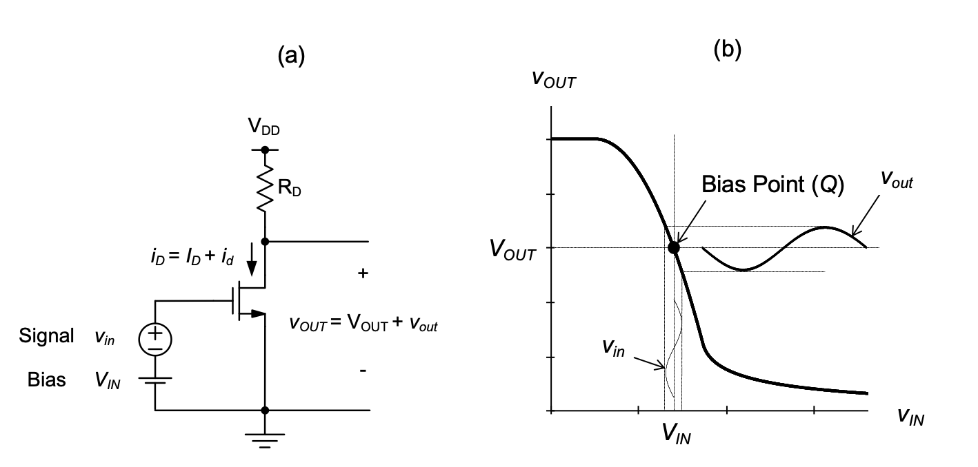
Per IEEE convention, the total quantity in such a decomposition is denoted using a lowercase symbol and uppercase subscript, i.e., \(v_{IN}\) = \(V_{IN}\) + \(v_{in}\) in our example. Similarly, the drain current is decomposed as \(i_{d}\) = \(I_{D}\) + \(i_{d}\), where \(I_{D}\) is the current at the operating point, and id captures the current deviations due to the applied signal.
Figure 2.10(b) elucidates this setup further using the circuit’s transfer characteristic. With \(v_{in}\) = 0, the output is equal to \(V_{OUT}\), which is called the bias point or operating point of the output node. The bias point is sometimes also called the quiescent point (Q), since the corresponding voltage level corresponds to that of a “quiet” input. Note that \(V_{OUT}\) can be calculated by evaluating Equation 2.13, as done previously.
With some nonzero \(v_{in}\) applied, the output will now see an excursion away from the bias point. For example, applying a positive \(v_{in}\) will result in a negative incremental change \(v_{out}\) at the output. How can we compute \(v_{out}\) for a given \(v_{in}\)? Since Equation 2.13 must hold for the total quantities \(v_{IN}\) = \(V_{IN}\) + \(v_{in}\) and \(v_{OUT}\) = \(V_{OUT}\) + \(v_{out}\) we can write
\[ V_{OUT}= V_{DD}-R_D\cdot \frac{1}{2}\mu_n C_{ox}\frac{W}{L}(v_{IN}-V_{Tn})^2 \tag{2.17}\]
or
\[ V_{OUT} + v_{out} = V_{DD}-R_D\cdot \frac{1}{2}\mu_n C_{ox}\frac{W}{L}(V_{IN} + v_{in} -V_{Tn})^2 \tag{2.18}\]
In order to simplify this expression, and since we are only interested in the change of \(v_{out}\) as a function of \(v_{in}\), it is useful to eliminate the constant term from this expression, given by
\[ V_{OUT}= V_{DD}-R_D\cdot \frac{1}{2}\mu_n C_{ox}\frac{W}{L}(V_{IN}-V_{Tn})^2 \tag{2.19}\]
After subtracting Equation 2.19 from Equation 2.18 and rearranging the terms, we obtain
\[ v_{out} = -R_D \mu_n C_{ox} \frac{W}{L}(V_{IN} - V_{Tn}) \cdot v_{in} [ 1+ \frac{v_{in}}{2(V_{IN} - V_{TN})}] \tag{2.20}\]
Using the drain current expression of Equation 2.7, and by defining
\[ V_{OV} = (V_{GS} - V_{Tn})|_{Q} = V_{IN} - V_{Tn} \tag{2.21}\]
the result can be further simplified and rewritten as
\[ v_{out} = -\frac{2I_D}{V_{OV}}\cdot R_D \cdot v_{in}(1+\frac{v_{in}}{2V_{OV}}) \tag{2.22}\]
where \(I_D\) is the transistor’s drain current at the bias point, and \(V_{OV}\) is introduced as a symbol for the quiescent point gate overdrive voltage.
From the end result in Equation 2.22, we see that \(v_{out}\) is a nonlinear function of \(v_{in}\). This is not surprising, since we are employing a transistor that exhibits a nonlinear I-V characteristic. While this derivation was relatively simple, the analysis of nonlinear circuits in general tends to be complex. Picture a circuit that contains several transistors, as for instance a cascade connection of several stages of the amplifier circuit considered here. Even with only a few nonlinear elements, most cases involving practical circuits with just moderate complexity tends to yield unwieldy expressions. A widely used solution to this problem is to approximate the circuit behavior using a linear model around its operating point, which we will discuss next.
2.2.4 The Small-Signal Approximation
Equation 2.22 is written in a format that suggests an opportunity for simplification. Provided that \(v_{in}\) \(\ll\) \(v_{OV}\), the bracketed term is close to unity and we can write
\[ v_{out} = -\frac{2I_D}{V_{OV}}\cdot R_D \cdot v_{in} = A_v \cdot v_{in} \tag{2.23}\] where \(A_v\) is a constant voltage gain term that relates the incremental input and output voltages.
Interestingly, the term Av can also be found using basic calculus. Assuming that the incremental voltages represent infinitesimally small deviations in the total signal, we can rewrite Equation 2.23 as
\[ dv_{OUT} = A_v \cdot dv_{IN} \tag{2.24}\]
and therefore
\[ A_v= \left. \frac{dv_{OUT}}{dv_{IN}} \right|_Q = \left. \frac{dv_{OUT}}{dv_{IN}} \right|_{v_{IN}=v_{IN}} \tag{2.25}\]
where the derivative is evaluated at the circuit’s operating point \(Q\) that is fully defined by choice of the input bias voltage \(V_{IN}\). By applying Equation 2.25 to Equation 2.17, we find
\[ A_v = \frac{d}{dv_{IN}} \left[ V_{DD} - R_D - \frac{1}{2} \mu_n C_{ox} \frac{W}{L} (v_{IN} - V_{Tn})^2 \right] \bigg|_{v_{IN} = v_{IN}} \]
\[ = -R_D \mu_n C_{ox} \frac{W}{L} (v_{IN} - V_{Tn}) \bigg|_{v_{IN} = v_{IN}} \tag{2.26}\]
\[ = -R_D \mu_n C_{ox} \frac{W}{L} (V_{IN} - V_{Tn}) = -R_D \mu_n C_{ox} \frac{W}{L} V_{OV} \]
Finally, using Equation 2.7, we find
\[ A_v = -\frac{2I_D}{V_{OV}}\cdot R_D \tag{2.27}\]
which is the same result obtained previously. The voltage gain \(A_v\) can be interpreted graphically as shown in Figure 2.11. From Equation 2.25 and basic calculus we know that \(A_v\) is the slope of the tangent to the transfer characteristic at the point (\(V_{IN}\), \(V_{OUT}\)), which is the operating point of the circuit.
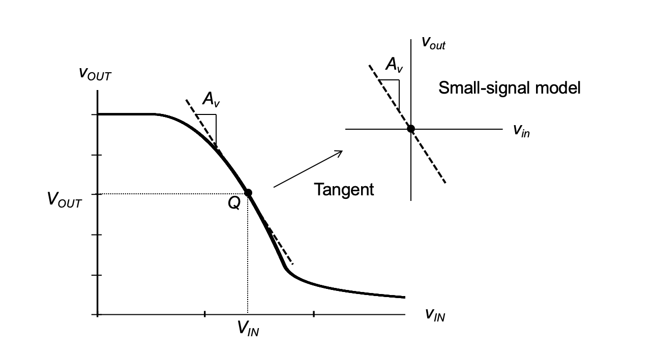
In analog circuit nomenclature, \(A_v\) is called the small-signal voltage gain of the circuit; this emphasizes that this quantity is only suitable for calculations with “small” signals such that nonlinear effects are negligible. In the particular circuit considered here, “small” means \(v_in\) \(\ll\) \(V_{OV}\), as seen from our analysis. The general concept of approximating circuit behavior by assuming small-signal excursions around an operating point is called small-signal approximation. In order to clearly distinguish a circuit transfer characteristic obtained through such an approximation from one that incorporates the nonlinear transistor behavior (e.g., Equation 2.17), the term large-signal transfer characteristic is typically used for the latter.
As we shall see in the remainder of this module, working with small-signal approximations greatly simplifies analog circuit analysis and design. The price paid for the approximation, however, is that the resulting equations by themselves cannot be used to reason about the circuit’s behavior for large signals, as for instance signals where \(v_{in}\) is comparable to, or even greater than, \(V_{OV}\). As illustrated in Figure 2.11, the small-signal approximation essentially creates a new coordinate system that linearly relates the input and output voltages. In this model, the output voltage follows the input linearly, no matter how large the applied voltage is. In reality, considering the circuit’s large signal transfer characteristic, signal clipping and strong waveform distortion can occur for large excursions and poorly chosen bias points. Examples of such cases are illustrated in Figure 2.12.
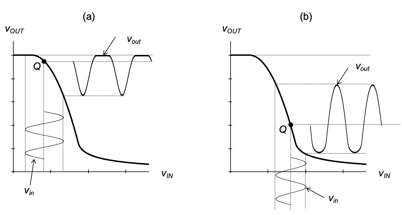
Example 2-4 : Signal clipping
Consider the circuit of Figure 2.10, using the parameters from Example 2-2(b): \(V_{DD}\) = 5 \(V\), \(R_D\) = 10 \(kΩ\), W/L = 10, and \(V_{IN}\) is adjusted to 1.5 V, so that \(V_{OUT}\) = 2.5 \(V\) at the circuit’s operating point. Calculate the most negative excursion that the incremental input voltage \(v_{in}\) can assume before the output is “clipped” to \(V_{DD}\) (as in Figure 2.12(a)).
SOILUTION
The circuit’s output voltage is given by
\[ v_{OUT} = V_{DD}-R_D\cdot \frac{1}{2}\mu_n C_{ox}\frac{W}{L}(V_{IN} + v_{in} -V_{Tn})^2 \]
Clipping \(v_{OUT}\) to the supply voltage implies \(v_{OUT}\) = \(V_{DD}\). This requires
\[ 0= V_{IN} + v_{in} - V_{Tn} \]
\[ v_{in} = -(V_{IN} - V_{Tn}) = - (V_{OV}) \]
\[ v_{in} = -(1.5V-0.5V) = -1V \]
In words, applying a negative signal (\(v_{in}\)) at the input of magnitude larger than 1 V will cause the output to reach the supply voltage. Making \(v_i\) more negative will create a “plateau” in the output waveform as shown in Figure 2.12(a).
In a majority of analog circuits, it is sufficient to use the large-signal characteristic for bias-point and signal-range calculations. For all other purposes, as for instance voltage gain calculations, it is usually appropriate and justifiable to work with small-signal approximations. Without this clever split in the analysis, most analog circuits of only moderate complexity would not be amenable to hand analysis, simply because the nonlinear nature of the transistors would create prohibitively complex systems of non- linear equations.
Circuits that are designed to amplify small signals from a transducer are classical examples where the small-signal approximation works. Consider, for instance, the above-discussed amplifier circuit fed with an input signal from a radio antenna, which is often on the order of several hundred microvolts. As long as \(V_{OV}\) is chosen larger than several hundred millivolts, the small signal approximation will hold with reasonable accuracy. Other examples (not covered in this module) include amplifiers that rely on electronic feedback, which tends to minimize the signal excursions around a circuit’s bias point (see Reference 2).
As a final remark, it should be noted that even if the input to a circuit is “small,” the output will always show at least some amount of nonlinear distortion. In our basic amplifier, this distortion is caused by the bracketed term in Equation 2.22. In cases where even weak distortion is an issue, the designer often employs computer simulation tools to study the relevant behavior. From a design perspective, deviations from linearity can be minimized if needed. For the discussed common-source amplifier, this is seen from Equation 2.22: decreasing the ratio \(v_{in}\) / \(V_{OV}\), either by reducing \(v_{in}\) or by increasing \(V_{OV}\) will result in improved linearity.
The exact analysis ofThe exact analysis of nonlinear distortion is beyond the scope of this module, and is typically treated only in advanced integrated circuit texts, as for instance Reference 3. We will focus here primarily on studying the relevant behavior of analog circuits using a linear small-signal abstraction, aided by basic bias-point and signal-range calculations.
2.2.5 Transconductance
The method of differentiating a circuit’s large-signal transfer characteristic to obtain a small-signal approximation was straightforward for the simple one-transistor circuit discussed so far. Unfortunately, for a larger circuit it is usually much more difficult and often tedious to derive a complete transfer characteristic in the form of Equation 2.17.
A clever workaround that is predominantly used in analog circuit analysis is based on linearizing the circuit element-by-element around the operating point. This method is applied in three steps: (1) Compute all node voltages and branch currents at the operating point using the devices’ large-signal model. (2) Substitute linear models for all nonlinear components and compute their parameters using the operating point information. (3) Compute the desired transfer function using the linear model obtained in step 2.
The biggest advantage of this method, called small-signal analysis, is that it avoids computing the large-signal transfer characteristic of the circuit, and instead defers the transfer function analysis until all elements have been approximated by linear models. The linearized models of nonlinear elements, such as MOSFETs, are typically called small-signal models.
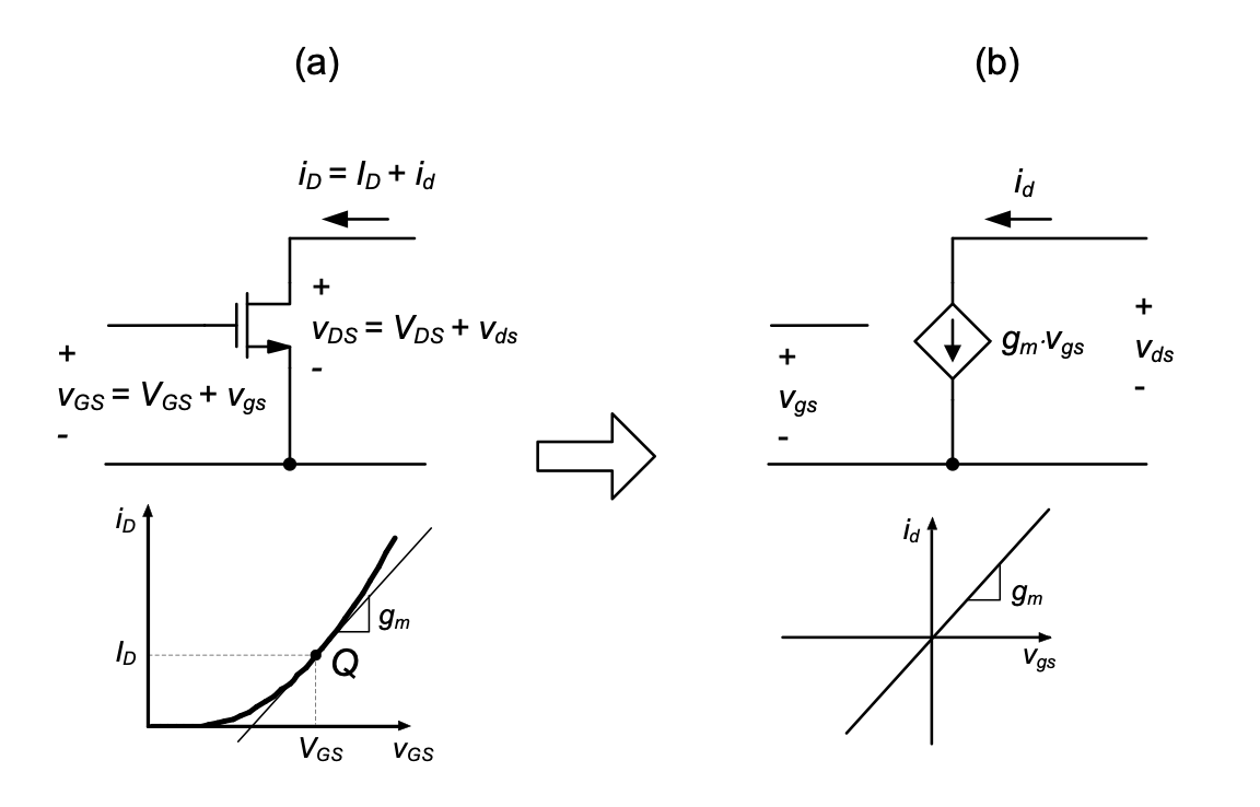
We will now illustrate the small-signal analysis approach by applying it to the basic common-source amplifier example covered so far in this chapter. Consider first the MOSFET device in Figure 2.7(a). In general, once the operating point of the transistor is known, the small-signal model is obtained by differentiating the large signal I-V relationships at this point. This is further illustrated in Figure 2.13, assuming that the MOSFET is biased in the saturation region. The proportionality factor that links the incremental drain current (\(i_d\)) and the gate-source voltage (\(v_{gs}\)) is given by the slope of the tangent to the large signal transfer characteristic at the bias point. This quantity is called transconductance, or \(g_m\). Mathematically, we can write
\[ g_m = \frac{i_d}{v_{gs}} = \left. \frac{di_D}{dv_{GS}} \right|_{v_{GS}=V_{GS}} \tag{2.28}\]
In order to find the transconductance for the saturation region of the device, we evaluate Equation 2.28 using Equation 2.7. This yields
\[ g_m = \mu_n C_{ox}\frac{W}{L}(V_{GS}- V_{Tn}) = \mu_n C_{ox}\frac{W}{L}V_{OV} \tag{2.29}\]
Alternative forms of this expression are obtained by eliminating \(V_{OV}\) or \(μ_n C_{ox}\) W/L using Equation 2.7, which gives
\[ g_m = \sqrt{2\mu_n C_{ox} \frac{W}{L}I_D} \tag{2.30}\]
or
\[ g_m = \frac{2I_D}{V_{OV}} \tag{2.31}\]
All of the above equations can be used to calculate \(g_m\); the choice of which equation is used depends on the given parameters. The physical unit for transconductance is \(A/V\) = \(Ω^{-1}\), or Siemens (\(S\)).
Once the transconductance is determined, we can insert the model of Figure 2.13(b) into the original circuit (Figure 2.7(a)) for further analysis. The resulting small-signal circuit equivalent is shown in Figure 2.14. No modeling modification is needed for the resistor \(R_D\), as it is already assumed in Figure 2.7(a) that it follows a linear \(I/V\) law (\(V= I \cdot R\)). However, since the supply voltage is constant in the large-signal model, it must be replaced with 0 V or ground (\(GND\)) in the small-signal model. This is because the differentiation of a constant quantity yields zero.

Using the model of Figure 2.14, we now apply Kirchhoff’s laws at the output and find \[ v_{out} = -g_m \cdot v_{in} \cdot R_D \tag{2.32}\]
Finally, by substituting Equation 2.31 we obtain
\[ v_{out} = -\frac{2I_D}{V_{OV}} \cdot R_D \cdot v_{in} = A_v \cdot v_{in} \tag{2.33}\]
As expected, this result is equivalent to what was obtained by applying the small-signal approximation to Equation 2.22, and also by differentiating Equation 2.17 at the operating point. However, as indicated previously, the big advantage of working with a small-signal model for individual transistors is that this simplifies the analysis of larger circuits.
2.2.6 P-Channel Common-Source Voltage Amplifier
As shown in Figure 2.15(a), we can also build a CS amplifier using a p-channel device. Similar to the n-channel case, we can derive a large-signal transfer characteristic using Equation 2.11 and by applying \(KVL\) at the output node. The resulting plot is shown in Figure 2.15(b). Compared to the n-channel case (Figure 2.7(b)), one can show that the characteristic is flipped sideways (since \(V_{SG}\) = \(V_{DD}\) - \(V_{IN}\)) and upside down (because \(I_D\) is negative for a p-channel transistor). Therefore, for small \(V_{IN}\) near 0 \(V\), the device operates in the triode region and the output voltage is close to \(V_{DD}\). For \(V_{IN}\) = \(V_{DD}\), the device is off and the output is at 0 \(V\), since \(V_{SG}\) = 0 and no current flows in the device.
In terms of its small-signal model, it follows that the p-channel CS amplifier is identical to the n-channel version. This can be seen intuitively by comparing Figure 2.7(b) and Figure 2.15(b): in the region around point \(B\), both transfer characteristics exhibit a negative slope and therefore will behave alike for small perturbations. We will show this formally in the following discussion.
We begin by inserting a small-signal model for the transistor as shown in Figure 2.16(a). Based on the positive variable convention of Equation 2.11, we define the transconductance for the p-channel transistor as
\[ g_m = \left. \frac{d}{dv_{SG}}((-i_D))\right |_Q \]
\[ = \mu_p C_{ox}\frac{W}{L}(V_{SG} + V_{Tp}) \tag{2.34}\]
\[ = \frac{2(-I_D)}{V_{SG}+V_{Tp}} = \frac{2(-I_D)}{V_{OV}} \]
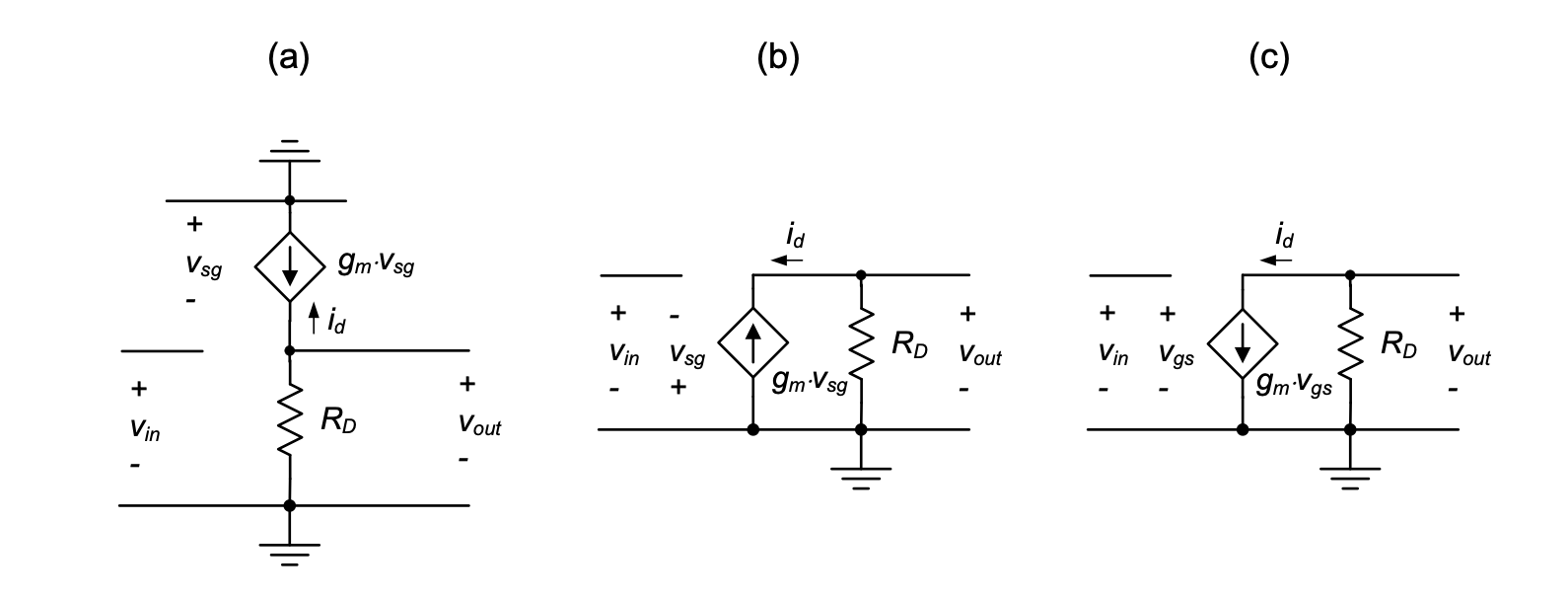
Note that through this expression, we have defined \(V_{OV}\) for the p-channel case as \(V_{SG}\) + \(V_{Tp}\), which is a positive quantity for a p-channel device in the “ON” state.
Although we could solve for the small-signal voltage gain directly with the circuit shown in Figure 2.16(a) it is easier to flip the transistor 180° (Figure 2-15(b)) so that the circuit appears similar to the n-channel version. Since \(v_{sg}\)=–\(v_{gs}\) we can change signs at the input and the dependent current source and find that the p-channel common-source amplifier small-signal model is identical to the n-channel version as shown in Figure 2.16(c).
This result applies more generally to all the transistor configurations and model extensions that we will study in this module. Once the operating point parameters of a p-channel device have been determined (e.g., a calculation of \(g_m\) using Equation 2.34), it is perfectly valid to replace it with an n-channel equivalent. This is a very powerful and convenient result, since it allows us to focus on n-channel only configurations in small-signal analyses, without having to worry about the specific sign conventions of p-channels.
2.2.7 Modeling Bounds for the Gate Overdrive Voltage
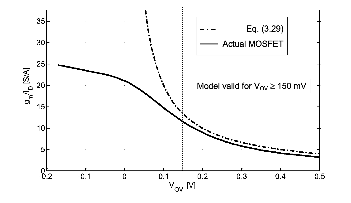
According to Equation 2.31, \(g_m/I_D\) = \(2/V_{OV}\) tends to infinity as the gate overdrive voltage \(V_{OV}\) approaches zero. This implies that for a transistor that is “barely on,” we can extract very large transconductance values for only small bias currents. Unfortunately, this behavior is incorrect, and stems from limitations of the device model discussed in Section 2-1. As \(V_{OV}\) approaches zero, a more complex analysis is needed to predict the drain current and its derivative with respect to gate voltage see Reference 4.
Figure 2.17 plots the \(g_m/I_D\) characteristic of a MOSFET, and the expected behavior based on Equation 2.31. As we can see, for \(V_{OV} < 150 mV\), a large discrepancy exists between a physical device and the prediction based on the simple square-law model used in this treatment. In order to avoid unrealistic design outcomes due to this modeling limitation, we define a bound for the minimum allowed gate overdrive voltage for all circuits covered in this module
\[ V_{OV}≥ V_{OVmin} = 150 mV \tag{2.35}\]
Designing with a smaller \(V_{OV}\) would require a more elaborate model for hand calculations, which is beyond the scope of this module. The interested reader is referred to advanced material on this topic, available for example in References 4 and 5.
2.2.8 Voltage Gain and Drain Biasing Considerations
In the basic common-source amplifier discussed so far, the drain resistor \(R_D\) serves a dual purpose: (1) it translates the device’s incremental drain current (\(i_d\)) into a voltage (\(V_{out}\)), and (2) it supplies the quiescent point drain current (\(I_D\)) for the MOSFET. As we shall show next, this creates an undesired link between the bias point constraints of the circuit and the achievable small-signal voltage gain of the amplifier. To see this, we rewrite Equation 2.36 as shown below
\[ A_v = - \frac{2I_D}{V_{OV}} \cdot R_D = -2\frac{V_R}{V_{OV}} \tag{2.36}\]
where \(V_R\) = \(V_{DD} – V_{OUT}\) is the voltage drop across RD at the operating point. This result leads to several interesting conclusions. First, note that the voltage gain of the amplifier is fully determined once \(V_{OV}\) and voltage drop across \(R_D\) are known. For example, if the circuit is biased such that \(V_{OV}\) = 0.2 \(V\) and \(V_R\) = 2 \(V\), we have \(A_v\) = –20; regardless of the particular W, L or \(\mu_n\) \(C_{ox}\) of the employed MOSFET. Second, since the possible values for \(V_{OV}\) are lower-bounded (Equation 2.35) and \(V_R\) is upper-bounded (finite \(V_{DD}\)), there exists a maximum possible \(A_v\) that can be obtained
\[ |A_{vmax}| = 2\frac{V_{Rmax}}{V_{OVmin}} = 2\frac{V_{DD}-V_{OVmin}}{V_{OVmin}} ≅ 2\frac{V_{DD}}{V_{OVmin}} \tag{2.37}\]
In this result, it was assumed the transistor is biased at the edge of the triode region, a somewhat impractical, but appropriate limit case to consider. Evaluating the above expression for \(V_{DD}\) = 5 V and \(V_{OVmin}\) = 150 \(mV\) yields \(|A_{vmax}|\) ≅ 67. Can we overcome this limit and change our amplifier such that it can achieve voltage gains beyond this value?
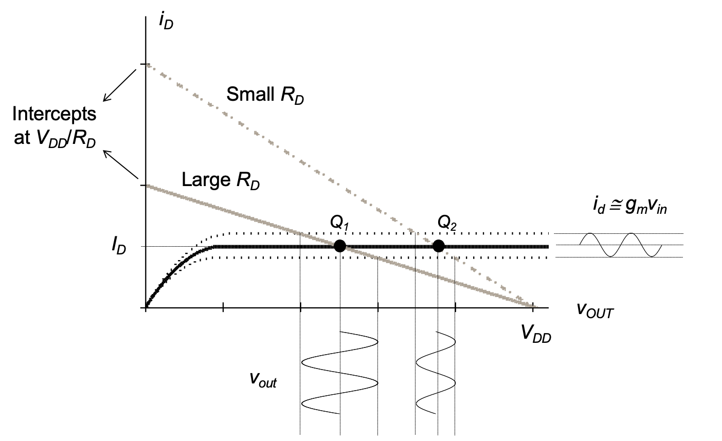
In order to investigate this, consider the load line illustrations shown in Figure 2.18. As explained in Section 2-2-2, the load line for our circuit is defined by the points (0, \(V_{DD}\)/\(R_D\)) and (\(V_{DD}\), 0). From the location of these points, we see that the x-axis intercept of the load line is fixed, while the y-intercept moves lower with larger values of \(R_D\). This reduces the slope of the load line, resulting in a larger small-signal voltage gain of the circuit. Furthermore, note that for a fixed quiescent point drain current \(I_D\), larger \(R_D\) shifts the output bias point \(V_{OUT}\) to smaller values, i.e., closer to the edge of the MOSFET’s triode region. This observation captures the result of Equation 2.37 in a graphical way: we cannot increase the small-signal voltage gain beyond a certain limit due the link between \(V_{OUT}\) and the chosen \(R_D\).
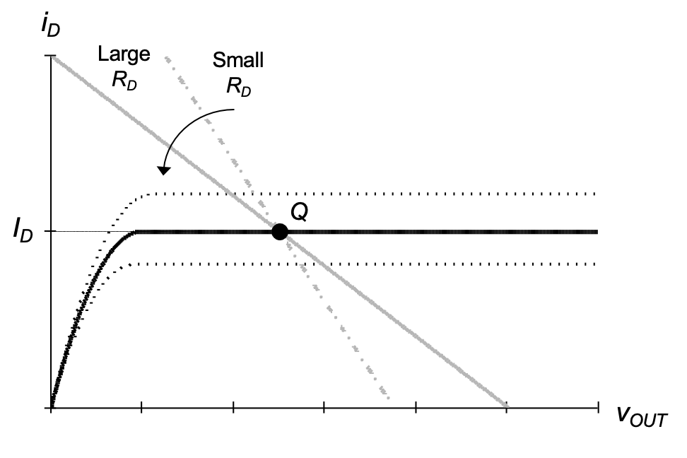
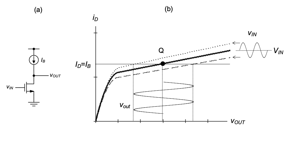
A more ideal situation is depicted in Figure 2.19. If we could somehow create a load line that “rotates” about the desired operating point (as a function of \(R_D\)), the voltage gain could be set independently of \(V_{OUT}\). A modified drain network that lets us achieve this behavior is shown in Figure 2.20(a). In this circuit, \(R_D\) is now connected to a voltage \(V_B\) (instead of the supply voltage \(V_{DD}\)) and an ideal current source \(I_B\) is used to provide a fixed current. In a realistic implementation circuit, \(I_B\) can be built, for example, using a p-channel MOSFET that operates in saturation. For the time being, we will neglect such implementation details, and postpone the discussion of current sources to Chapter 5.
With this new configuration, the relationship between \(i_D\) and \(v_{OUT}\) becomes
\[ i_D = I_B = \frac{V_B - v_{OUT}}{R_D} \tag{2.38}\]
or \[ v_{OUT} = V_B + (I_B - i_D)R_D \tag{2.39}\]
As we can see from these equations (also graphically shown in Figure 2.20(b)), at the point \(v_{OUT}\) = \(V_B\), we have \(i_D\) = \(I_B\), regardless of the value of \(R_D\)$. Therefore, utilizing this point as the operating point of our amplifier precisely achieves the goal we have in mind. In particular, we wish to set \(I_B\) = \(I_D\), the desired quiescent point drain current of the MOSFET, and \(V_B\) = \(V_{OUT}\), the desired output operating point. With this choice, the role of the current source is to provide the MOSFET’s bias current, while the resistor RD is responsible only for converting the incremental drain current into an incremental output voltage; no DC bias current flows in this element.
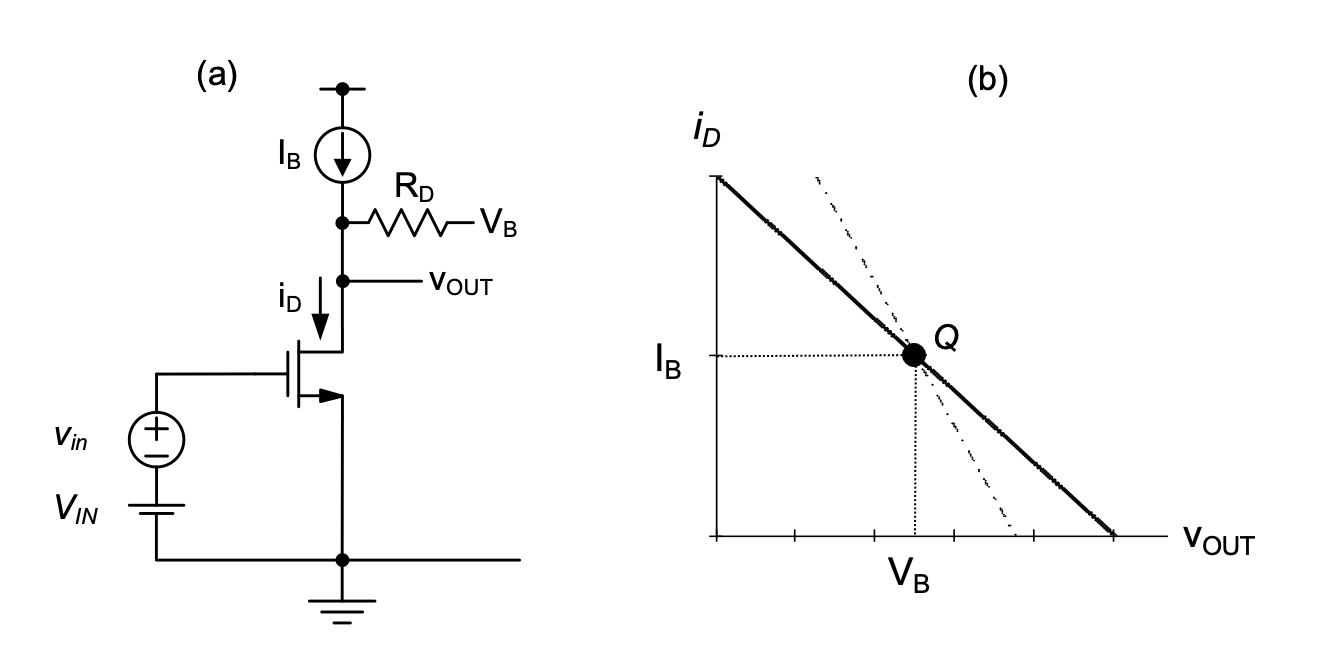
Since the voltage source \(V_B\) and the current source \(I_B\) aid in maintaining the circuit’s bias point, we generally classify these elements as biasing sources. However, it is important to distinguish their function from the input bias voltage \(V_{IN}\). \(V_{IN}\) directly sets the quiescent point gate-source voltage of the transistor and therefore fully defines the operating point on the MOSFET’s I-V characteristic and the corresponding drain current. In the above-described scenario, \(I_B\) is adjusted to supply this same drain current, but does not define it. We therefore categorize \(I_B\) an auxiliary bias current that helps sustain, but does not set the quiescent point of the transistor. Since \(V_B\) defines the quiescent point output voltage of the circuit, we refer to this element as the output bias voltage.
Lastly, it is important to note that for the modified circuit in Figure 2.20(a), the previously derived small-signal model shown in Figure 2.14 still applies. This can be understood by differentiating Equation 2.39 at the operating point to find the small-signal equivalent of the network placed at the drain of the amplifier
\[ \left. \frac{dv_{out}}{di_D} \right|_Q = \frac{d}{di_D}(V_B +(I_B - i_D)R_D) = -R_D \tag{2.40}\]
As this result indicates, and as we have seen previously, any constant sources, such as \(V_B\), \(I_B\), etc., drop out of the small signal model, which captures only components that affect the incremental changes in currents and voltages around the circuit’s operating point.
For the circuit in Figure 2.20(a), one might now be tempted to think that we can obtain an arbitrarily large voltage gain, as long as \(R_D\) is made very large. Unfortunately this is not the case for several reasons, the first of which stems from physical effects that we have not yet included in the MOSFET model. This aspect is further discussed in Section 2-3. In addition, there are practical limitations to the attainable voltage gain, discussed next.
2.2.9 Sensitivity of the Bias Point to Component Mismatch\(^*\)
Consider a CS amplifier biased at the gate as done previously with a bias voltage \(V_{IN}\), directly setting up the quiescent point drain current \(I_D\) (depending on \(W/L\) and other relevant device parameters). Our goal in using the drain bias network of Figure 2.20(a) is then to set \(I_B\) = \(I_D\) and chose \(VB\) such the output is biased at a reasonable, desired \(V_{OUT}\). Unfortunately, in practice, we can never achieve \(I_B\) = \(I_D\) exactly; there will always be a non- zero \(ΔI\) = \(I_B\) – \(I_D\). This case is shown in Figure 2.21. As illustrated, the finite \(ΔI\) leads to a shift \(ΔV\) away from the desired output operating point \(V_B\). This shift is proportional to \(R_D\), since the current difference \(ΔI\) flows into \(R_D\), creating the undesired \(ΔV\).
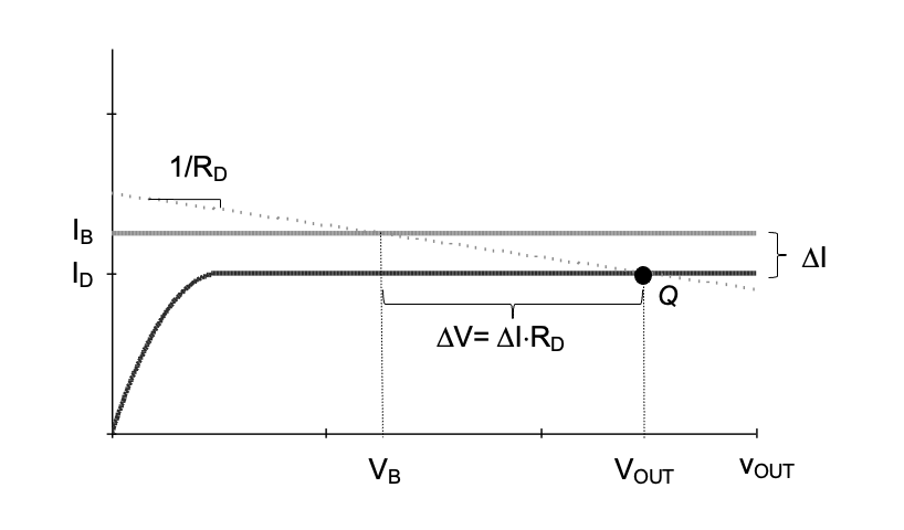
Example 2-5: Output Bias Voltage Shift due to Current Mismatch
Consider the CS amplifier of Figure 2.20(a), biased at the gate such that \(V_{OV}\) = 500 mV. Assume \(I_D\) = 200 \(μA\), and that \(R_D\) is chosen such that the amplifier achieves \(A_v\) = –400. Considering Figure 2.21, how much mismatch between \(I_B\) and \(I_D\) (in \(%\)) can be tolerated such that \(V_{OUT}\) deviates from the intended bias point (\(V_B\)) by no more than \(ΔV\) = 500 \(mV\)? Repeat this calculation for \(A_v\) = –40 and –4.
SOLUTION
We begin by computing the transconductance of the MOSFET
\[ g_m = \frac{2I_D}{V_{OV}} = \frac{2 \cdot 200\mu_A}{0.5V} = 800 µS \]
In order to achieve \(A_v\) = –400, we require \(R_D\) = 400/800 \(μS = 500 kΩ\). Therefore,
\[ \frac{∆ I}{I_D} = \frac{∆V}{I_D R_D} < \frac{500 mV}{200\mu A \cdot 500kΩ} = 0.5 \% \]
For \(A_v\) = –40 and \(A_v\) = –4, the result modifies to 5%, and 50%, respectively.
As expected, this result confirms that for larger \(|A_v|\), the auxiliary bias current \(I_B\) must match the MOSFETs drain current more accurately. How precisely can we match these two currents? Unfortunately, answering this question in detail is beyond the scope of this module, and is the subject of advanced research papers such as Reference 6. Nonetheless, it can be said in general that matching currents, voltages, or any other electrical quantities in today’s integrated circuits to better than 1% requires special care and understanding. In some cases, even 10% matching can be hard to guarantee. With this guideline in mind, it becomes clear that the circuit of Figure 2.20(a) may become impractical if we aim for too much voltage gain.
The general issue of properly dealing with variability in integrated circuit components is a complex topic that is still being actively researched. At the introductory level of this module, the main point that the reader should retain is that any circuit whose bias point relies on precisely matched components or high absolute accuracy in any electrical parameter may not be robust in the presence of component variability. In general, experienced circuit designers avoid situations that resemble the “balancing of a marble on the tip of a cone,” i.e., circuits that will be overly sensitive to variations in component parameters. We will take up this point once more when discussing practical biasing circuits in Chapter 5.
As a final note concerning the issue of variability, it is worth mentioning that electronic feedback can help alleviate problems as the one analyzed in Example 2-5. Picture for example adding an auxiliary circuit to Figure 2.20(a) that somehow measures VOUT, and adjusts \(V_{IN}\) (and therefore \(I_D\)) until the desired output operating voltage is set. In such schemes, relatively large variations in \(I_B\) can be absorbed. Feedback circuits are not covered in this module, but are the subject of advanced texts such as Reference 2.
2.3 Channel Length Modulation
The MOSFET model used so far assumes that the drain current in the saturation region is independent of the drain-source voltage. This behavior corresponds to that of an ideal current source, which is generally non-physical. A more realistic output characteristic observed in real MOSFETs is shown in Figure 2.22. For a physical MOSFET, \(I_D\) tends to increase with \(V_{DS}\); an effect that can be explained (to first-order) as a voltage dependent modulation of the channel length (see Section 2-3-1).
When inserted into the circuit of Figure 2.20(a), the dependence of drain current on \(v_{DS}\) (\(v_{OUT}\)), will have an impact on the overall transfer characteristic of the amplifier, which we will thus consider in this section. For simplicity, let us first investigate the case of \(R_D\) –> ∞, i.e., no explicit drain resistance, and using only an ideal current source in the drain biasing network (see Figure 2.23(a)). In this case, the load line is horizontal at \(I_B\) = \(I_D\), as shown in Figure 2.23(b). As before, the operating point \(Q\) is established at the point where the load line and the device’s drain characteristic for the applied quiescent point input voltage (\(V_{IN}\)) meet.
Note that similar to the case considered in the previous section, the output operating point voltage in this circuit will shift by large amounts for relatively small changes in \(I_B\) (or MOSFET parameters). This issue must be addressed when this circuit is used in practice, for example by providing a feedback mechanism that adjusts \(I_B\) such that the desired \(V_{OUT}\) is maintained in the presence of component variations.
Assuming that a well-defined operating point has been established by some means, incremental changes in \(v_{IN}\) applied around the bias point \(Q\) will force the intersection of the horizontal load line with the MOSFET’s drain characteristics to move sideways (since the drain current cannot change), creating a finite output voltage excursion vout. The magnitude of this voltage excursion, and thus the voltage gain of the circuit, depends on the slope of the MOSFET’s drain characteristic in saturation. The voltage gain achieved in this configuration is commonly called the intrinsic voltage gain of the MOSFET, as it represents the voltage gain of the transistor by itself, without any added resistances in the drain bias network. By the same reasoning, the circuit of Figure 2.23(a) is often called the intrinsic voltage gain stage. The voltage gain and other parameters of more complex amplifier circuits are often directly related to the intrinsic voltage gain of their constituent transistors, giving this parameter a fundamental significance in circuit design.
2.3.1 The \(\lambda\)-Model
Unfortunately, the intrinsic voltage gain of a MOSFET cannot be predicted using the MOSFET model established so far. We will therefore extend the first-order MOSFET model to incorporate the dependence of the saturation current on the drain-source voltage. As a first step, we will describe the effect in terms of large-signal equations. Next, we will apply a small-signal approximation that makes it possible to capture the \(I_{Dsat} – V_{DS}\) dependence through a single resistor added to the MOSFET’s small-signal model.
We begin by revisiting an approximation that was made in Section 2-1. In order to arrive at the constant drain current expression in saturation (Equation 2.7), it was assumed that \(ΔL\), the distance from the pinch-off point to the drain, is negligible relative to the channel length L. In reality, this approximation is fine only as long we do not care about the \(I_D-V_{DS}\) dependence seen in Figure 2.22. Therefore, in order to get a quantitative handle on the MOSFET’s intrinsic voltage gain, we must further investigate the impact of the physics at the drain side.
The simplest possible way to proceed is to factor \(ΔL\) into the existing derivation of Section 2-1. Instead of integrating Equation 2.5 over the length L, we use \(L– ΔL\) as the upper limit of the integral. Recall that \(L– ΔL\) is the actual location where the mobile charge vanishes, i.e., \(Qn(y)= 0\). With this change we obtain the following expression for the saturation region.
\[ I_D = \frac{1}{2} \mu_n C_{ox} \frac{W}{L-∆L} ({V_{GS}} - V_{Tn})^2 \tag{2.41}\]
Now, provided that \(ΔL\) is still small (but not negligible) relative to \(L\), we can apply the following first-order approximation:
\[ \frac{1}{L-∆L} ≈ \frac{1}{L}(1+\frac{∆L}{L}) \tag{2.42}\]
Next, note that \(ΔL\) must be a function of the drain voltage, since the depletion region widens with increasing reverse bias. This effect is commonly called channel length modulation. Unfortunately, an exact calculation of \(ΔL\) as a function of the terminal voltages involves solving the two-dimensional Poisson equation and leads to complex expressions. For simplicity, we assume that the fractional change in channel length is proportional to the drain voltage
\[ \frac{∆L}{L} = \lambda_n V_{DS} \tag{2.43}\]
where \(\lambda_n\) is the channel length modulation parameter. Device measurements and simulations indicate that \(\lambda_n\) approximately varies with the inverse of the channel length. For the MOSFETs in this module, we will use
\[ \lambda_n = \frac{0.1\mu mV^(-1)}{L} \tag{2.44}\]
where \(L\) is in \(\mu_nm\). Finally, we substitute Equation 2.44 and Equation 2.43 into Equation 2.41 and find a very useful approximation to the drain current in saturation, often called the \(\lambda\)-model:
\[ I_D = \frac{1}{2} \mu_n C_{ox} \frac{W}{L} ({V_{GS}} - V_{Tn})^2 (1+\lambda_n V_{DS}) \tag{2.45}\]
where \(V_{DS}\) ≥\(V_{DSsat} = V_{GS}-V_{Tn}\). This model has proven useful and sufficiently accurate for basic hand calculations, even though the physics related to the \(I_{DSsat}\)-\(V_{DS}\) dependence are in reality much more complex than discussed above. As long as \(\lambda_n\) is determined from measurements or accurate physical analysis, the model properly approximates a typical MOSFET’s I-V characteristic to first-order. Higher-order models are typically not used in hand analysis, but find their use in advanced computer simulation models.
We now wish to incorporate the channel length modulation effect into the small-signal model of the MOSFET. An important new feature that must be considered in this task is that the drain current of Equation 2.45 now depends on two voltages, namely \(V_{DS}\) and \(V_{GS}\). A common and appropriate way of handling this situation for small-signal modeling is to approximate the incremental drain current around the operating point as the total differential (as frequently used in error analysis) due to both variables, i.e.
\[ i_d = \left. \frac{∂ i_D}{∂ V_{GS}}\right |_Q \cdot v_{gs} + \left. \frac{∂ i_D}{∂ V_{GS}}\right |_Q \cdot v_{ds} \tag{2.46}\]
The above expression essentially treats \(v_{DS}\) as a constant when evaluating the derivative of \(i_D\) with respect to \(v_{GS}\). Similarly, \(v_{GS}\) is assumed constant in the differentiation with respect to \(v_{DS}\). This use of partial differentiation is justified and reasonably accurate as long as at least one of the following two conditions is met:
The excursion in the variable that is treated as a constant can be approximated as infinitesimally small and therefore negligible.
The excursion in the variable that is approximated as a constant is considerable, but nonetheless does not affect the derivative with respect to the second variable.
In the context of a common-source amplifier, for instance, the first condition applies to \(v_{GS}\). Just as in the derivation of the simple small-signal model without \(V_{DS}\) dependence, we can argue that changes in \(v_{GS}\) are suitably modeled as “small” (relative to \(V_{OV}\)). The same condition cannot be applied to \(v_{DS}\) in general. Often times the output voltage, and therefore \(v_{DS}\), see large excursions in amplifier circuits. In order for Equation 2.46 to be reasonably accurate, we must require the second condition, i.e., the derivative of \(i_D\) w.r.t. \(v_{GS}\) must not strongly depend on drain-source voltage. By inspection of Equation 2.45, we see that this condition is met as long as \(\lambda_n\) is small, which is typically the case for MOSFETs intended for use in amplifier stages.
To continue with our analysis, we rewrite Equation 2.46 as \[ i_d = g_m v_{gs} + g_o v_{ds} \tag{2.47}\]
where \[ g_m = \left. \frac{∂ i_D}{∂ V_{GS}}\right |_Q = \mu_n C_{ox} \frac{W}{L} ({V_{GS}} - V_{Tn}) (1+\lambda_n V_{DS}) = \frac{2I_D}{{V_{GS}} - V_{Tn}} = \frac{2I_D}{V_{OV}} \tag{2.48}\]
and \[ g_o = \left. \frac{∂ i_D}{∂ V_{GS}}\right |_Q = \frac{1}{2}\mu_n C_{ox} \frac{W}{L} ({V_{GS}} - V_{Tn})^2 \lambda_n = \frac{2I_D}{{V_{GS}} - V_{Tn}} = \frac{2I_D}{V_{OV}} \tag{2.49}\]
where the approximate end result assumes \(\lambda_n V_{DS}\) \(\ll\) 1, a condition that is often satisfied for long channels and moderate \(V_{DS}\). For instance, assuming L = 2 \(\mu\)m and \(V_{DS}\) = 2 \(V\) gives \(\lambda_nV_{DS}\) = 0.1 which is much less than one.
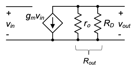
In the above expressions, \(g_m\) is the transconductance of the MOSFET (as defined previously) and go is called the output conductance. The inverse of go is called the output resistance, \(r_o\) = \(g_o^{-1}\). Graphically,the output conductance corresponds to the slope of the transistor’s drain characteristic at the operating point, which is the derivative of \(i_D\) with respect to \(v_{DS}\), while keeping the gate-source voltage constant (see Figure 2.24(a)). In the small-signal model of the MOSFET, the output conductance can be included as shown in Figure 2.24(b). This representation follows directly from Equation 2.47, which represents Kirchhoff’s Current Law equation for the drain node of the transistor.
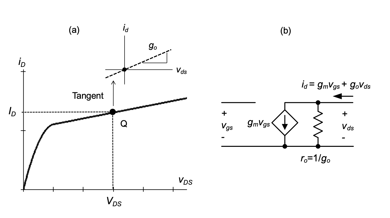
Just as with the simple \(g_m\)-only small-signal model of Figure 2.13, the main idea for the usage of the extended model with go is to use the small-signal equivalent circuit of Figure 2.24(b) in a larger circuit. We will illustrate this using two examples of interest: the intrinsic voltage gain stage of Figure 2.23(a) and the common-source amplifier of Figure 2.20(a).
2.3.2 Common-Source Voltage Amplifier Analysis Using the \(\lambda\)-Model
For the intrinsic voltage gain stage, the small-signal model of Figure 2.24(b) corresponds directly to the small-signal model for the entire circuit with \(v_{in} = v_{gs}\) and \(v_{out} = v_{ds}\). Therefore, the voltage gain of the intrinsic gain stage is given by
\[ A_v = -\frac{g_m}{g_o} = - g_m r_o ≅ - \frac{2I_D}{V_{OV}} \cdot\frac{1}{\lambda_n I_D} = - \frac{2}{\lambda_n V_{OV}} \tag{2.50}\]
From this expression, we can see that the voltage gain can be increased by increasing \(L\), which will decrease \(\lambda\). Alternatively, the voltage gain can be increased by reducing \(V_{OV}\), which corresponds to reducing the drain current \(I_D\) for a fixed aspect ration \(W/L\). In this context, note that for \(V_{OV}\) → 0, Equation 2.50 predicts infinite voltage gain. This non-physical outcome stems from the same issue already discussed in Section 2-2-7: for $V_{OV} → 0, \(g_m\) approaches infinity for a fixed current in our simplistic square-law I-V model. As argued before, the usable range for \(V_{OV}\) must therefore be lower-bounded as specified in Equation 2.35. Assuming \(V_{OV} = V_{OVmin}\) = 150 \(mV\) and L = 1 \(μm\), the intrinsic voltage gain of a MOSFET described by the parameters used in this module is approximately 2/(0.1·0.15) = 133.
Let us now consider the common-source amplifier of Figure 2.20(a). Including the finite output conductance from the \(\lambda\)-model, the small-signal model is modified as shown in Figure 2.25 and the voltage gain expression becomes
\[ A_v = -g_m \left( \frac{1}{r_o} + \frac{1}{R_D} \right)^{-1} = -g_m R_{out} \tag{2.51}\]
For \(R_D\) → \(∞\) , the small signal voltage gain approaches the intrinsic voltage gain as given by Equation 2.50. For \(R_D \ll r_o\), we can approximate \(A_v ≅ –g_m R_D\). More generally, without even knowing the exact values of \(r_o\) and \(R_D\), we can argue that as long as the desired gain is much less (in magnitude) than the intrinsic voltage gain, \(r_o\) can be neglected in the voltage gain calculation. To see this, we can rewrite Equation 2.51 as
\[ \frac{1}{|A_v|} = \frac{1}{g_m r_o} + \frac{1}{g_m R_D} \]
\[ g_m R_D = \frac{|A_v|}{1 - \frac{|A_v|}{g_m r_o}} ≅ |A_v| \quad \text{for} \quad |A_v| \ll g_m r_o \tag{2.52}\]
Example 2-6: Analysis of a CS Amplifier Using the \(\lambda\) -Model
Consider the CS voltage amplifier of Figure 2.20(a) with \(W\) = 80 \(μm\), \(L\) = 2 \(μm\) and \(R_D\) = 50 \(kΩ\). The gate is biased such that \(V_{OV} = 500 mV\) and \(V_B\) is set to 2 \(V\), which is also the desired output operating point \(V_{OUT}\). Compute the required bias current \(I_B\) and the small-signal voltage gain of the circuit using the \(\lambda\)-model. Repeat the small-signal voltage gain calculation for \(R_D\) = 5 \(kΩ\).
SOLUTION
The bias current is found using
\[ I_B = I_D = \frac{1}{2} \mu_n C_{ox} \frac{W}{L} ({V_{GS}} - V_{Tn})^2 (1+\lambda_n V_{DS}) \]
\[ \frac{1}{2} \cdot 50 \frac{\mu A}{V^2} \cdot \frac{80}{2}(0.5V)^2(1+0.05 \cdot 2) \]
\[ = 275 \mu A \]
The corresponding transconductance and output resistance at the operating point are
\[ g_m = \frac{2I_D}{V_{OV}} = \frac{2 \cdot 275 \mu A}{0.5 V} = 1.1 mS \]
\[ r_o = \frac{1+\lambda_n V_{DS}}{\lambda_n I_D} = \frac{1+ 0.05 \cdot 2}{0.5V^{-1} \cdot 275\mu A} = 80 kΩ \]
According to Equation 2.51, the small signal voltage gain for \(R_D\) = 50 \(kΩ\) is given by
\[ A_v = -1.1mS (\frac{1}{80kΩ} + \frac{1}{50kΩ})^{-1} = -33.9 \]
for \(R_D\) = 5 \(kΩ\) we find
\[ A_v = -1.1mS (\frac{1}{80kΩ} + \frac{1}{5kΩ})^{-1} = -5.18 \]
Since the voltage gain for \(R_D\) = 5 \(kΩ\) is much less than the intrinsic voltage gain of the transistor (\(g_m r_o\) = 88), it is appropriate to neglect \(r_o\) in this calculation. We can simply compute
\[ A_v = -1.1 mS \cdot 5 kΩ = -5.5 \]
This result differs only by about 5.9% from the accurate calculation.
Another opportunity for useful engineering approximations in the application of the \(\lambda\)-model lies in the operating point calculation. We will illustrate this point through the example below.
Example 2-7: Approximate Operating Point Calculations
Recalculate \(I_D\), \(g_m\) and \(r_o\) by approximating \(\lambda\)\(V_{DS} ≅ 0\) in the large-signal bias point calculations. Also recalculate \(A_v\) for \(R_D\) = 50 \(kΩ\) using this approximation. Compare the results to the values obtained in Example 2-6.
SOLUTION
For \(\lambda\) \(V_{DS}\) ≅ 0, the bias current is estimated as
\[ I_B = I_D = \frac{1}{2} \mu_n C_{ox} \frac{W}{L} ({V_{GS}} - V_{Tn})^2 \]
\[ = \frac{1}{2} \cdot 50 \frac{\mu A}{V^2} \cdot \frac{80}{2}(0.5V)^2 \]
\[ = 250 \mu A \]
The corresponding transconductance and output resistance at the operating point are
\[ g_m = \frac{2I_D}{V_{OV}} = \frac{2 \cdot 250 \mu A}{0.5 V} = 1 mS \]
\[ r_o = \frac{1}{\lambda_n I_D} = \frac{1 }{0.5V^{-1} \cdot 250\mu A} = 80kΩ \]
and the voltage gain becomes
\[ A_v = -1mS (\frac{1}{80kΩ} + \frac{1}{50kΩ})^{-1} = -30.8 \]
Relative to the accurate calculation from Example 2-6 (\(A_v\) = –33.9), this result is in error by only about 9.1%.
There are several reasons why it is commonly acceptable to neglect the \(\lambda\)\(V_{DS}\) term in bias point hand calculations. First, without this approximation, the calculations can become cumbersome and lead to transcendental equations that are tedious and undesirable to solve in light of only a moderate percent-improvement in the obtained accuracy. If a more accurate result is desired, it can often be obtained more easily from computer simulations, which often follow a hand calculation in practice anyway. Last, one can argue that any circuit in which the operating point parameters strongly depend on \(\lambda\) may be impractical in the first place. The accuracy of the \(\lambda\)-model as far as absolute I-V values are concerned can only be approximate due to its empirical nature. For high accuracy analysis, much more complex models (such as the one described in Reference 7) must be used, carefully calibrated with physical measurements and subsequently evaluated in computer simulations. For the purpose of developing an introductory feel for circuits, however, the \(\lambda\)-model is still the most appropriate, mainly due its simplicity.
Table 2-3 summarizes the technology parameters introduced in this chapter.
| Parameter | n-channel MOSFET | p-channel MOSFET |
|---|---|---|
| Threshold voltage | \(V_{Tn}\) = 0.5V | \(V_{Tp}\) = -0.5V |
| Transconductance parameter | \(μ_nC_{ox}= 50μA/V^2\) | \(μ_pC_{ox}= 25μA/V^2\) |
| Chanel length modulation parameter | \(\lambda_n =0.1V^{-1}/L\) (L in \(\mu\) m) | \(\lambda_p =0.1V^{-1}/L\) (L in \(\mu\) m) |
2.4 Two-Port Model for the Common-Source Voltage Amplifier
The circuit shown in Figure 2.25 corresponds to a transconductance amplifier model (with voltage output) since we modeled the MOSFET as a voltage controlled current source, which is in line with its physical behavior in the saturation region. Alternatively, and since the circuit is meant to function as a voltage amplifier, we can equivalently model it using a native voltage amplifier two-port as shown in Figure 2.26. The reader can prove that for this model the open-circuit voltage gain is given by \(A_v\) = \(–g_m R_{out}\), where \(R_{out}\) corresponds to the parallel connection of \(R_D\) and \(r_o\). The native voltage amplifier model is sometimes preferred since it more directly expresses the intended function we assumed in this chapter. However, as we shall see in Chapter 3, the voltage amplifier two-port is no longer a convenient representation for the CS voltage amplifier when device capacitances are included.
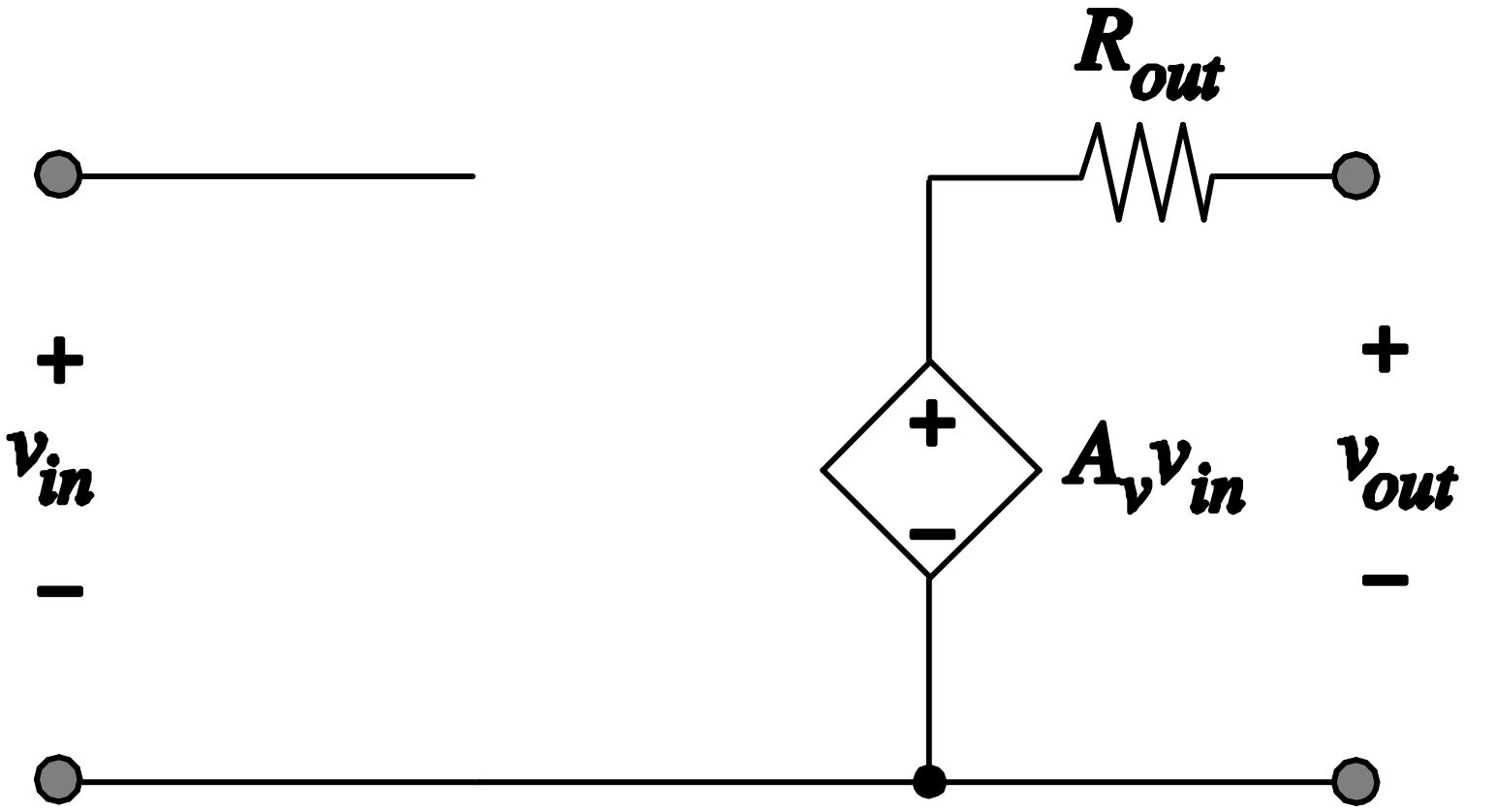
Figure 2.27 shows the small-signal commonsource voltage amplifier model together with an input transducer and load resistance. Since the input resistance of the CS amplifier is infinite, no resistive division takes place at the input port and \(v_{in} = v_s\). Thus, the overall voltage gain is computed as
\[ A'_v = \frac{v_{out}}{v_s} = A_v \cdot \left(\frac{R_L}{R_L + R_{out}}\right) \tag{2.53}\]
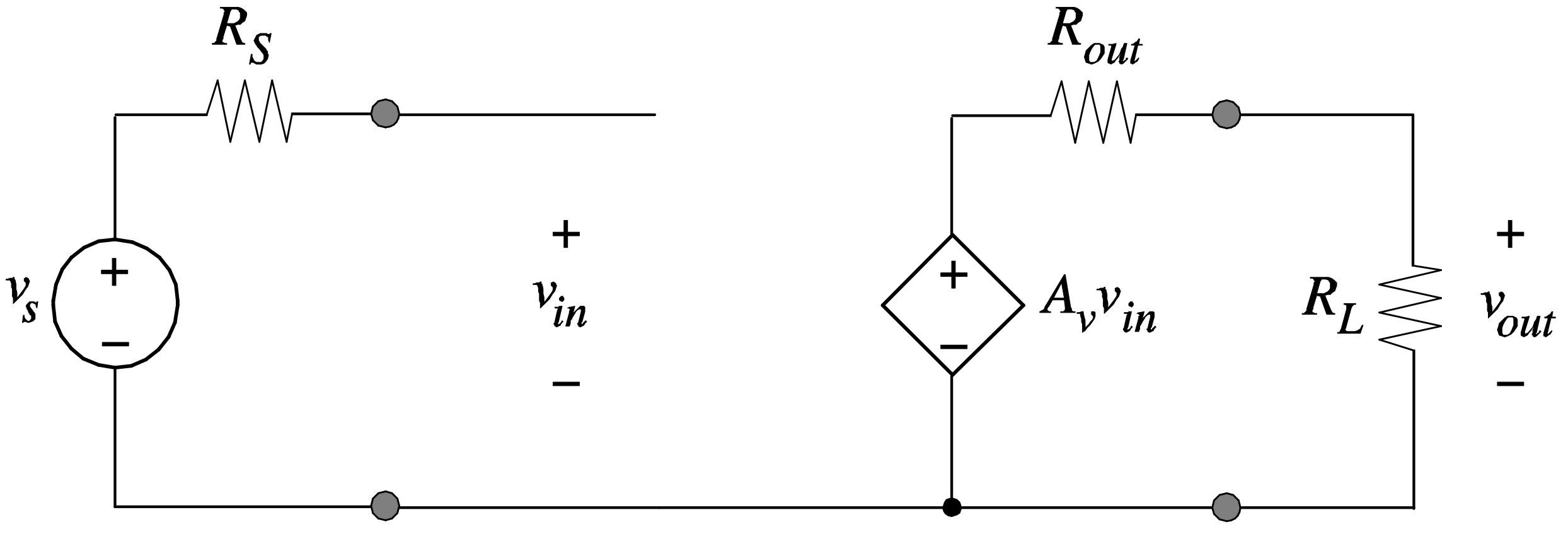
The same expression can be found from the circuit of Figure 2.25 with \(R_L\) included across the output port. The reader is invited to prove this.
As a final note, we should emphasize that adding a load resistance may have implications on the bias point of the circuit. For example, if the load resistor carries a DC current, this current will affect the quiescent point output voltage of the amplifier. In this case, the load resistance must also be connected to the circuit in the operating point analysis where the small-signal parameters such as \(r_o\) are computed. Problem 2-17 looks at an example.
2.5 Summary
In this chapter we reviewed the basic I-V characteristics of a MOSFET and employed this device to construct examples of common-source voltage amplifiers. In deriving a model for the MOSFET, we concentrated on first-order effects that define the transistor’s operation. The nonlinear nature of even the simplest device model dictates the use of small-signal approximations to enable analyses with manageable complexity. The presented methodology begins by finding the operating point of the transistor. Next, the small-signal equivalent is used to construct a linear small-signal model for further analysis.
We studied the basic common-source voltage amplifier with drain resistance and found that the voltage gain in this circuit is directly proportional to the voltage drop across the resistor, which imposes practical limits on the achievable voltage gain. A modified circuit based on an auxiliary bias current source was then analyzed as an alternative and used as a motivation to incorporate the effect of channel length modulation using the \(\lambda\)-model.
The most important concepts that you should have mastered are:
Determining MOSFET drain currents in all regions of operation; determining the regions of operation based on the transistor’s terminal voltages.
Constructing transfer characteristics and load line plots for common-source stages for various drain bias configurations.
Calculating the operating point of a CS stage and the MOSFET’s small-signal parameters \(g_m\) and \(r_o\).
Drawing the small-signal model of a CS stage and calculating its voltage gain.
2.6 References
R. F. Pierret, Semiconductor Device Fundamentals, Prentice Hall, 1995.
P. R. Gray, P. J. Hurst, S. H. Lewis, and R. G. Meyer, Analysis and Design of Analog Integrated Circuits, 5th Edition, Wiley, 2008.
D. O. Pederson and K. Mayaram, Analog Integrated Circuits for Communication: Principles, Simulation and Design, 2nd Edition, Springer,
Y. Tsividis, Operation and Modeling of the MOS Transistor, 2nd Edition, McGraw-Hill, New York, 1999.
P. G. A. Jespers, The \(g_m/I_D\) Methodology, a Sizing Tool for Low-Voltage Analog CMOS Circuits, Springer, 2010.
M. J. M. Pelgrom, et al., “Matching properties of MOS transistors,” IEEE J. of Solid-State Circuits, pp. 1433-1439, May 1989.
G. Gildenblat, et al., “PSP: An Advanced Surface-Potential-Based MOSFET Model for Circuit Simulation,” IEEE Trans. Electron Devices, pp. 1979-1993, Sept. 2006.
2.7 Problems
Unless otherwise stated, use the standard model parameters specified in Table 2.3 for the problems given below. Consider only first-order MOSFET behavior and include channel length modulation (as well as any other second-order effects) only where explicitly stated.
P2.1 An n-channel transistor biased in saturation with \(W/L = 10\) carries a drain current of 200 \(\mu\)A when \(V_{GS}\) = 1.5 \(V\) is applied. With \(V_{GS}\) = 1 \(V\), the current drops to 50 \(\mu\)A. Determine \(V_{Tn}\) and \(\mu C_{ox}\) of this transistor.
P2.2 Show that two MOS transistors in series with channel lengths \(L_1\) and \(L_2\) and identical channel widths can be modeled as one equivalent MOS transistor with length \(L_1 + L_2\) (see Figure 2.28). Assume that \(M_1\) and \(M_2\) have identical parameters except for their channel lengths. Hint: there are (at least) two ways to solve this problem. One is through extensive algebra; the other is though physical insight and arguments based on the MOSFET cross-section.
P2.3 Derive an analytical expression for the input voltage that corresponds to the transition point (point \(C\)) between the saturation and triode regions in Figure 2.7(b).
P2.4 In Example 2-4, we calculated the most negative input excursion that the circuit in Figure 2.10 can handle before the output is clipped to the supply voltage. In this problem, calculate the most positive input excursion that can be applied before the MOSFET enters the triode region. Assume the same parameters as in Example 2-4: \(V_{DD}\) = 5 \(V\), \(R_D\) = 10 \(kΩ\), W/L = \(10\), and \(V_{IN}\) is adjusted to 1.5 \(V\), so that \(V_{OUT}\) = 2.5 \(V\) at the circuit’s operating point.
P2.5 For the circuit shown in Figure 2.29, sketch \(v_{OUT}\) as a function of \(v_{IN}\). Assume that \(v_{IN}\) varies from 0 to 5 \(V\). There is no need to carry out any detailed calculations; simply draw a qualitative graph and mark pertinent asymptotes and breakpoints (such as changes in the MOSFETs region of operation).
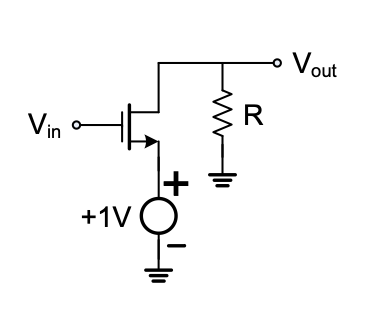
P2.6 Derive the small-signal voltage gain given by Equation 2.27 through direct differentiation of Equation 2.17, i.e., apply 2.25.
P2.7 A field effect transistor built using a new (fictitious) material behaves “almost” exactly like a conventional MOSFET in silicon technology. The large signal I-V characteristic (in the saturation region) is given by
\[ I_D = \frac{1}{2} \mu_n C_{ox} \frac{W}{L} ({V_{GS}} - V_{Tn})^{2.5} \]
Assuming that \(\mu C_{ox} W/L\) = 100 \(\mu A\)/\(V^{2.5}\) and \(I_D\) = 1 \(\mu\)A,
compute the transconductance of the device.
P2.8 The ratio of the small-signal drain current excursion and quiescent point drain current (\(i_d/I_D\)) is sometimes called the drain modulation index. Show that for a MOSFET, \(i_d/I_D\) is twice as large as the relative excursion in the gate-source voltage, \(v_{gs}/V_{OV}\).
P2.9 Consider the CS amplifier shown Figure 2.10(a). Calculate the small-signal voltage gain assuming \(V_{IN}\) = 1.5 \(V\), W/L = 20, \(R_D\) = 5 \(kΩ\), and \(V_{DD}\) = 5 \(V\). Be sure to check the device’s region of operation.
P2.10 Consider the p-channel CS amplifier shown in Figure 2.15(a). Assuming \(W/L\) = 20, \(R_D\) = 5 \(kΩ\), and \(V_{DD}\) = 5 \(V\), calculate the required quiescent point input voltage so that \(V_{OUT}\) = 2.5 \(V\). What is the small-signal gain of the circuit?
P2.11 Repeat Problem 2.9 with \(R_D\) = 10 \(kΩ\). With this value, the MOSFET operates in the triode region. Compute the small-signal voltage gain by writing the large-signal relationship between the input and output for the triode region and subsequent differentiation at the operating point.
P2.12 Consider the cascade connection of two CS amplifiers as shown in Figure 2.30.
Draw the small-signal equivalent model for this circuit.
Calculate the small-signal voltage gains \(v_{out1}/v_{in}\) and \(v_{out2}/v_{in}\). Assume that \(V_{IN} = V_{DD} / 2\) and that the device sizes are chosen such that the bias points of nodes \(v_{out1}\) and \(v_{out2}\) are also exactly at \(V_{DD} / 2\) .
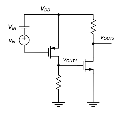
P2.13 Repeat Problem 2.9 and include the effect of channel length modulation in the small-signal voltage gain calculation. Neglect channel length modulation in the bias point calculation. Quantify the percent difference in the calculated small-signal voltage gain compared to Problem 2.9. Assume that the channel length of the MOSFET is 2 \(\mu\)m.
P2.14 For the p-channel common-source amplifier shown in Figure 2.15(a)
Given \(W/L= 12\) \(\mu m\)/2 \(\mu m\) and \(R_D\) = 10 \(kΩ\), calculate \(V_{IN}\) such that \(V_{OUT}\) is 2.5 \(V\). \(V_{DD}\) = \(5V\). Neglect channel length modulation in this calculation.
What is the small-signal voltage gain, \(A_v = v_{out} /v_{in}\) ? Include the effect of channel-length modulation in your calculation.
To increase the voltage gain, you increase \(R_D\) to 100 \(kΩ\). Calculate the new small-signal voltage gain, \(A_v\). You must re-bias the circuit so that \(V_{OUT}\) = 2.5 \(V\).
We could also try to increase the voltage gain of the initial circuit by increasing \(W/L\) rather than \(R_D\). Calculate the new \(A_v\) if \(W/L\)= 120 \(\mu m\) /2 \(\mu m\) and \(R_D\) = 10 \(kΩ\). Be sure to re-bias the circuit so that \(V_{OUT}\) = 2.5 \(V\).
P2.15 Calculate the small-signal gain of the intrinsic gain stage shown in Figure 2.23(a), assuming \(W\)= 10 \(\mu m\) and using the parameters given below. In each case, explicitly calculate the gate overdrive voltage (\(V_{OV}\)), the transconductance (\(g_m\)) and the output resistance (\(r_o\)). Assume that the circuit is biased such that the MOSFET operates in the saturation region. Neglect \(V_{DS}\) dependence in the calculation of \(r_o\) .
\(I_D\) = 100 \(\mu\)A, \(L\) = 2 \(\mu\)m
\(I_D\) = 50 \(\mu\)A, \(L\) = 2 \(\mu\)m
\(I_D\) = 100 \(\mu\)A, \(L\) = 4 \(\mu\)m
P2.16 Consider the CS amplifier of Figure 2.20(a) with the following parameters: \(V_B\) = 2.5 \(V\), \(I_B = 500\,\mu\text{A}, \; W = 20\,\mu\text{m}, \; L = 1\,\mu\text{m},\) and \(R_D\) = 5 \(kΩ\) .
Calculate the exact value of \(V_{IN}\) required such that \(I_D = I_B\), and \(V_{OUT} = V_B\). Include the effect of channel length modulation in your calculation.
Using the value of \(V_{IN}\) found in part (a), re-compute \(V_{OUT}\) for the two cases when \(\lambda\) changes by +50% and -50%, respectively. Such discrepancies may be due to variations in the semiconductor process or simply due to uncertainty in the simplistic \(\lambda\)-model.
P2.17 Consider the CS amplifier shown in Figure 2.31 with the following parameters: \(V_{DD}\) = 5 \(V\), \(V_{IN}\) = 1.8 \(V\), W = 15 \(\mu m\), L = 1 \(\mu m\), \(R_D\) = 5 \(kΩ\), and \(R_L\) = 10 \(kΩ\).
Calculate the output quiescent point voltage and drain current of the circuit, taking the connected load resistance \(R_L\) into account. Ignore channel-length modulation in this calculation.
Calculate \(g_m\) and \(r_o\) using the parameters from part (a). Take \(V_{DS}\) dependence into account.
Draw a two-port voltage amplifier model for the circuit and calculate the open-circuit voltage gain (\(A_v\)) and overall voltage gain (\(A'_v\)) with the load resistor connected.
Repeat parts (a) and (b) without considering the connected \(RL\) and recompute the two-port parameters of part (c). Summarize the observed differences.